Electrooptic system array, charged-particle beam exposure apparatus using the same, and device manufacturing method

a technology of charged particle beam and electroderooptic system, applied in the direction of optical radiation measurement, instruments, therapy, etc., can solve the problems of low productivity, difficult operation of electron beams independently, orbit and aberration change, etc., to reduce crosstalk uniqueness, high precision, and high reliability

Inactive Publication Date: 2005-11-15
CANON KK
View PDF67 Cites 61 Cited by
  • Summary
  • Abstract
  • Description
  • Claims
  • Application Information

AI Technical Summary

Benefits of technology

[0008]The present invention has been made to overcome the conventional drawbacks, and has as its principal object to provide an improvement of the prior arts. It is an object of the present invention to provide an electrooptic system array which realizes various conditions such as downsizing, high precision, and high reliability at high level. It is another o...

Problems solved by technology

This method suffers many problems as a mass-production exposure apparatus because of a low throughput.
This method is advantageous to a simple repetitive pattern but disadvantageous to a random pattern such as a logic interconnection pattern in terms of the throughput, and a low productivity disables practical ap...

Method used


Image

  • Electrooptic system array, charged-particle beam exposure apparatus using the same, and device manufacturing method
  • Electrooptic system array, charged-particle beam exposure apparatus using the same, and device manufacturing method
  • Electrooptic system array, charged-particle beam exposure apparatus using the same, and device manufacturing method

Examples


Embodiment Construction

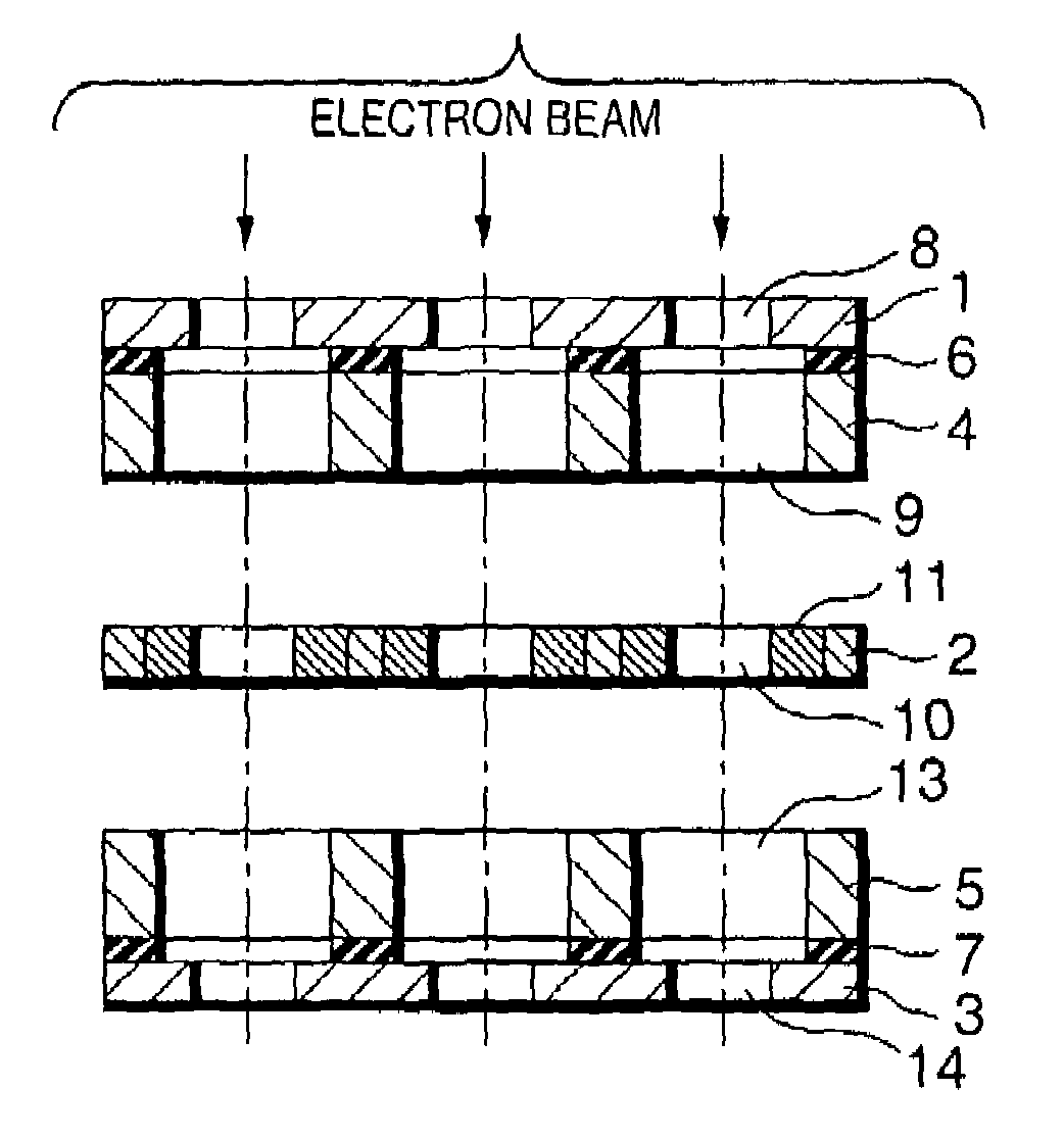
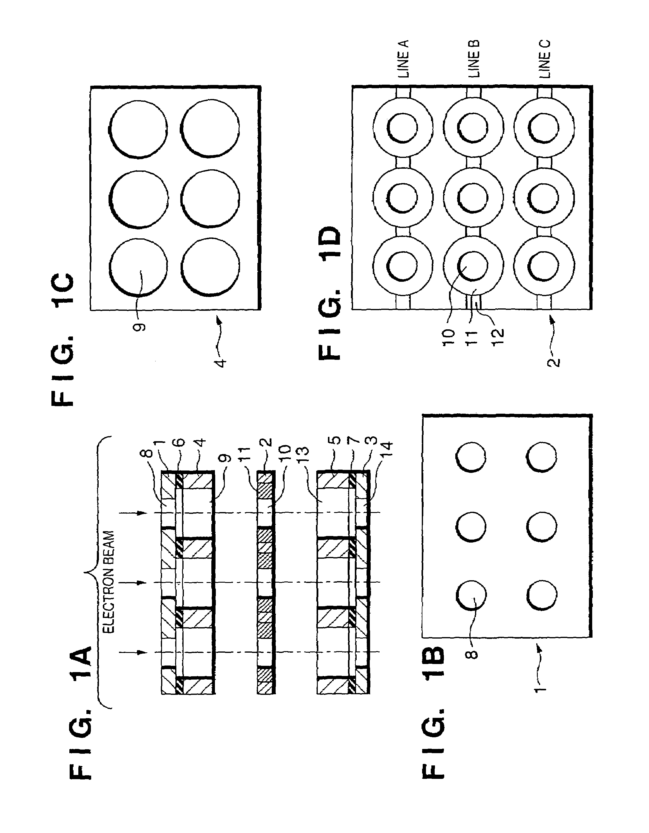
[0039]An electrooptic system array according to an embodiment of the present invention will be described. FIG. 1A is an exploded sectional view of the electrooptic system array. The electrooptic system array shown in FIG. 1A is constituted by sequentially stacking, on the paths of a plurality of electron beams (charged-particle beams), an upper electrode 1, upper shield electrode 4, middle electrode 2, lower shield electrode 5, and lower electrode 3, each of which has a plurality of apertures. FIG. 1B is a plan view of the upper electrode 1 when viewed from the top, FIG. 1C is a plan view of the upper shield electrode 4 when viewed from the top, and FIG. 1D is a plan view of the middle electrode 2 when viewed from the top.

[0040]The upper electrode 1 has a thin-film structure 10 μm in thickness that is formed from an electrode layer of a conductive material (e.g., Cu or Au), and has a plurality of 80-μm diameter circular apertures 8 arrayed regularly at a pitch of 200 μm. The lower e...


PUM


Abstract

This invention relates to an electrooptic system array having a plurality of electron lenses. The electrooptic system array includes upper, middle, and lower electrodes arranged along the paths of a plurality of charged-particle beams, the upper, middle, and lower electrodes having pluralities of apertures on the paths of the plurality of charged-particle beams, an upper shield electrode which is interposed between the upper and middle electrodes and has a plurality of shields corresponding to the respective paths of the charged-particle beams, and a lower shield electrode which is interposed between the lower and middle electrodes and has a plurality of shields corresponding to the respective paths of the charged-particle beams.

Description

FIELD OF THE INVENTION[0001]The present invention pertains to the technical field of an electrooptic system suitable for an exposure apparatus using charged-particle beams such as electron beams, and relates to an electrooptic system array having an array of a plurality of electrooptic systems.BACKGROUND OF THE INVENTION[0002]In production of semiconductor devices, an electron beam exposure technique receives a great deal of attention as a promising candidate of lithography capable of micro-pattern exposure at a line width of 0.1 μm or less. There are several electron beam exposure methods. An example is a variable rectangular beam method of drawing a pattern with one stroke. This method suffers many problems as a mass-production exposure apparatus because of a low throughput. To attain a high throughput, there is proposed a pattern projection method of reducing and transferring a pattern formed on a stencil mask. This method is advantageous to a simple repetitive pattern but disadv...

Claims


Application Information

Patent Timeline
IPC IPC(8): G01N23/00G03F7/20G21G5/00H01J37/305G21K5/10H01J37/02H01J37/04H01J37/12H01J37/10H01L21/02H01L21/027H01J37/24H01L31/00H01J9/14H01J9/18H01J37/30
CPCH01J9/14H01J9/18H01J37/12H01J37/3007G01N23/00H01J2237/1205H01J2237/151H01J2237/1534H01J2237/3175H01J2237/31774
Inventor ONO, HARUHITOMURAKI, MASATO
Owner CANON KK
Why Eureka
Try Eureka