

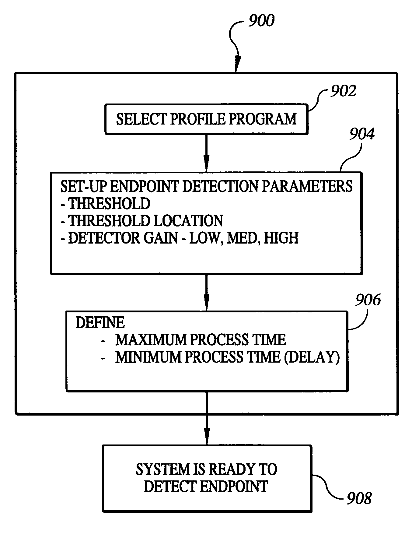
Full spectrum endpoint detection
- Summary
- Abstract
- Description
- Claims
- Application Information
AI Technical Summary
Benefits of technology
Problems solved by technology
Method used
Image

Examples
Embodiment Construction
)
[0049]In describing the preferred embodiment of the present invention, reference will be made herein to FIGS. 1–15 of the drawings in which like numerals refer to like features of the invention.
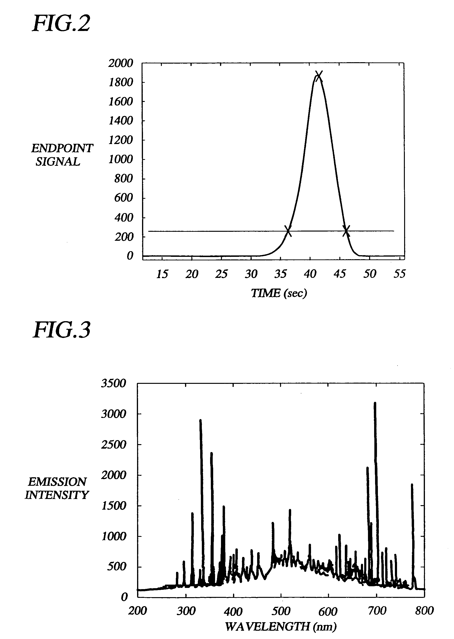
[0050]The present invention provides a powerful and easy-to-use endpoint detection system for semiconductor processing. The invention employs software algorithms and an assembly of readily available hardware. The preferred embodiment of this invention measures the intensity of light emitted by a process plasma as a function of wavelength and time, using optical emission spectroscopy (OES). The method of the invention is applicable to any detection method which provides a large number of process relevant data.
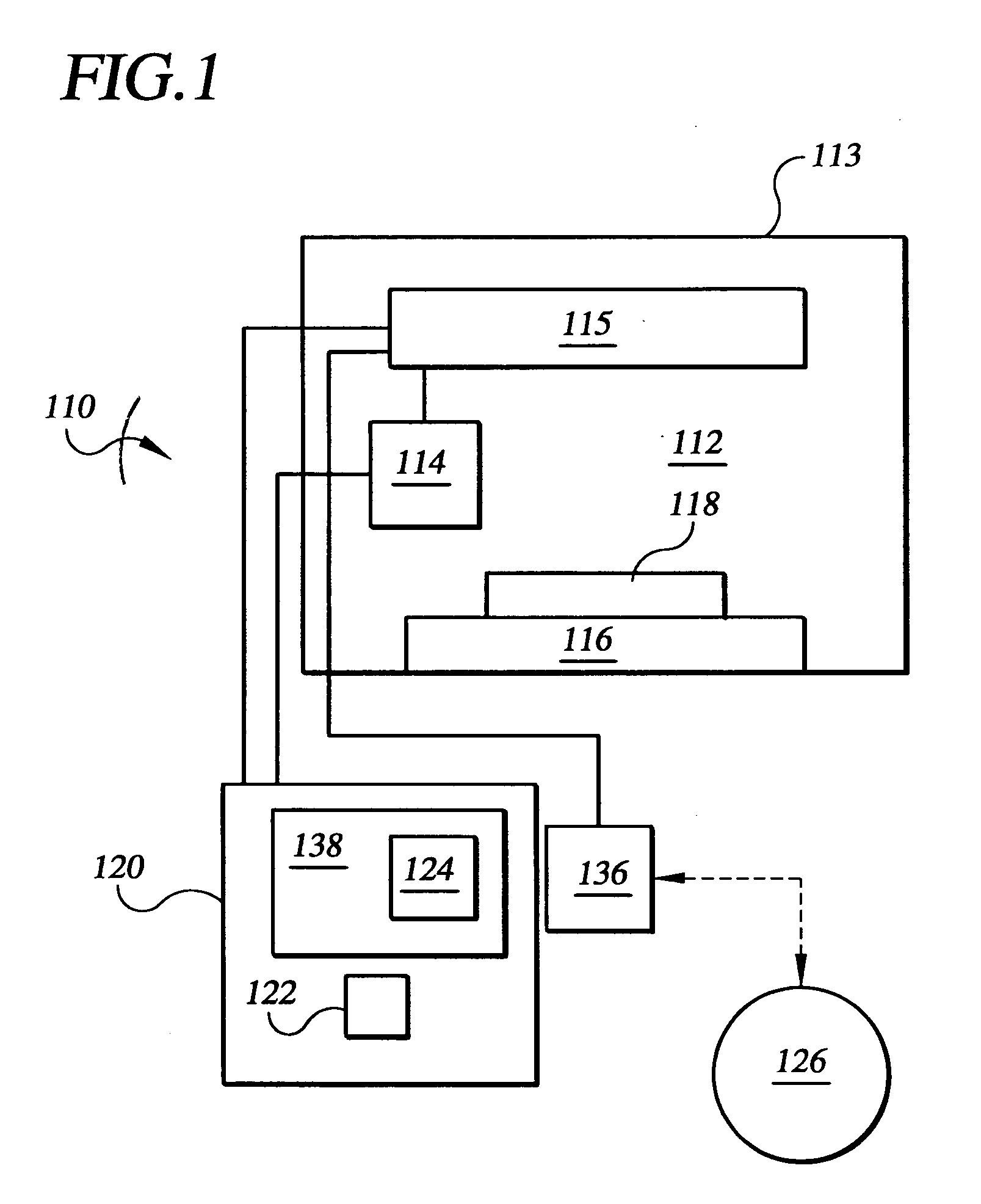
[0051]The system of the present invention preferably employs a device for detecting light emissions from a process plasma, which is, in the embodiment described herein, an optical emission spectrograph with a charge coupling device (CCD) array. The preferred system also includes a comput...
PUM
 Abstract
Description
Claims
Application Information