Method and device for providing a semiconductor etching end point and for detecting the end point

a technology of semiconductor etching and end point, which is applied in the direction of individual semiconductor device testing, semiconductor/solid-state device testing/measurement, instruments, etc., can solve the problems of difficult control, inability to achieve simple and effective etching stop, inaccurate, etc., and achieves economic benefits, cost-effectiveness, and sufficient precision

Inactive Publication Date: 2005-12-13
ROBERT BOSCH GMBH
View PDF12 Cites 10 Cited by
  • Summary
  • Abstract
  • Description
  • Claims
  • Application Information

AI Technical Summary

Benefits of technology

[0016]Thus, the device according to the present invention and the methods according to the present invention permit manufacturing of micromechanical structures that are very economical and sufficiently precise for many applications, in which expensive plasma sources are not necessary, and in which, above all, cost-effective process gases may be used.

Problems solved by technology

In practice, such masking layers are not measurably removed, so that even very deep or long silicon etchings are possible without the requirement for thick masking layers.
However, in using such a method for manufacturing micromechanical structures, such as cavities or diaphragms, a drawback is the fact that a simple and effective etching stop is missing.
This being the case, up to this point, a cavity to be generated in a silicon wafer was simply etched so deeply that a hole was created in the wafer, or the creation of a diaphragm or cavity having a defined thickness or depth was performed on a purely time-controlled basis, which is difficult to control and inaccurate.

Method used


Image

  • Method and device for providing a semiconductor etching end point and for detecting the end point
  • Method and device for providing a semiconductor etching end point and for detecting the end point

Examples


Embodiment Construction

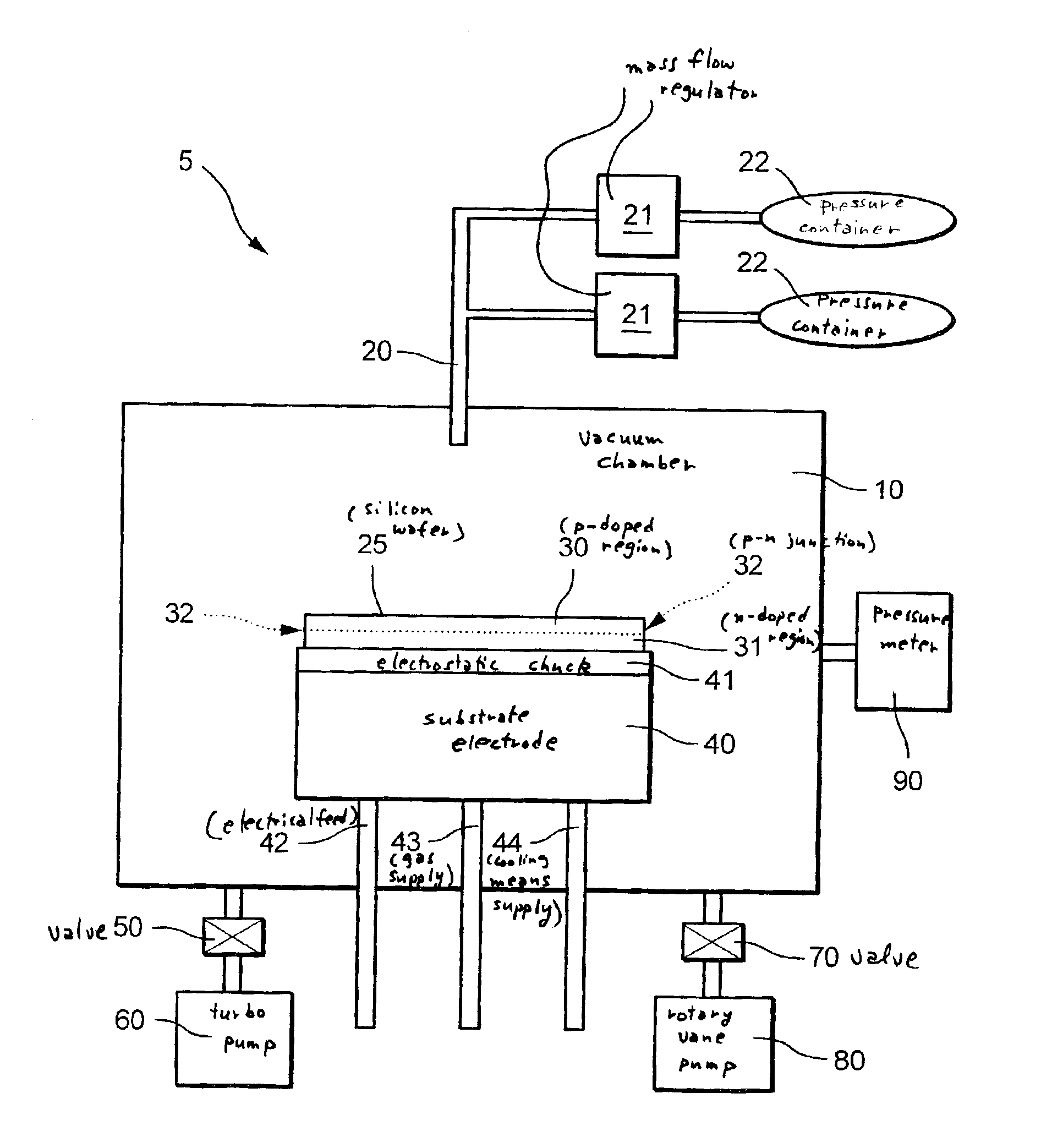
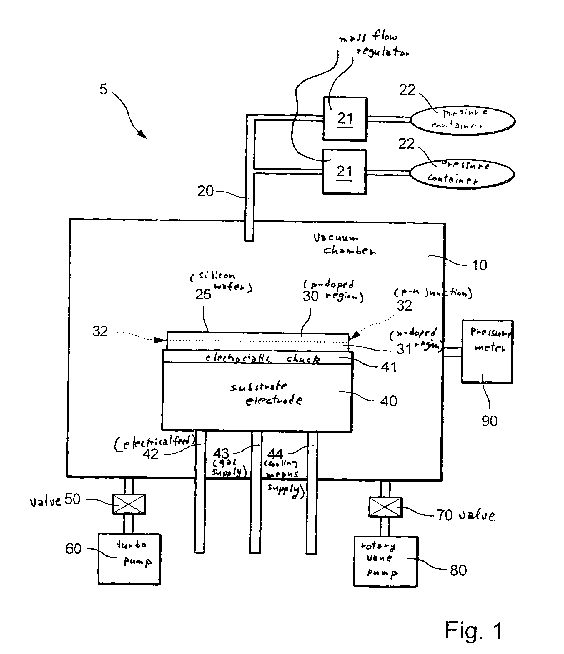
[0018]FIG. 1 shows an etching device 5 that is suitable for carrying out the method according to the present invention, having a vacuum chamber 10 and a gas inlet 20, the process gas(es) used being supplied to the vacuum chamber 10 from pressure containers 22 via post-connected mass flow regulators 21 via gas inlet 20. In the example explained, the process gas is ClF3, which has a sufficiently high vapor pressure to be supplied via usual mass flow regulators 21, or BrF3, in which case, because of its low vapor pressure of approximately 7 mbar at room temperature, special mass flow regulators 21 are required. By the way, in FIG. 1 it may also be provided that pressure containers 22 and / or the pipes and mass flow regulators 21 are heated, in order to avoid the formation of condensate and / or to increase the vapor pressure of process gas BrF3.

[0019]In vacuum chamber 10 used as the process chamber, a substrate electrode 40 is also provided, onto which a silicon wafer 25 is clamped as the...


PUM


Abstract

A method is provided for detecting an end point, a material transition or a boundary surface during the etching of a semiconductor element, a zone of the semiconductor element having non-homogeneous load carrier density and/or non-homogeneous load carrier polarity, particularly a p-n junction, which has an electrical voltage applied to it during etching, and an electrical current induced by it in this zone is measured, and reaching of this zone during etching is determined from a change in the electrical current. This method is suitable for the detection of the etching end point in gas phase etching, in particular with the aid of the etching gases ClF3 and/or BrF3, or in the anisotropic plasma etching of silicon substrates. In addition, a method is provided for etching a semiconductor element using a gaseous etching medium, during which the speed of removal of the semiconductor element is set or changed via a setting of the polarity and/or the density of free load carriers in the semiconductor element. In addition, a device for etching a semiconductor element, which device is suitable for carrying out the two methods described above, is provided.

Description

FIELD OF THE INVENTION[0001]The present invention relates to a method for recognizing an end point, a material transition or a boundary surface during the etching of a semiconductor element, in particular for etching end point recognition in gas phase etching of silicon substrates, as well as a method for etching a semiconductor element using a gaseous medium, and a device for etching a semiconductor element.BACKGROUND INFORMATION[0002]When using etching gases such as chlorine trifluoride (ClF3) or bromine trifluoride (BrF3), after the adsorption of these compounds on a silicon surface, by the liberation of fluorine radicals, which react with silicon atoms of the available silicon surface to form spontaneously volatile silicon fluoride compounds, which subsequently leave the surface, silicon is spontaneously etched. This being the case, silicon removal occurs in those places where silicon and the etching gas used come into contact with each other. In this connection, it is known tha...

Claims


Application Information

Patent Timeline
Patent Type & Authority Patents(United States)
IPC IPC(8): H01J37/32H01L21/00
CPCH01J37/32935H01L21/67069
Inventor BREITSCHWERDT, KLAUSLAERMER, FRANZ
Owner ROBERT BOSCH GMBH
Why Eureka
Try Eureka