Starter device for normally off JFETs

a silicon diode rectifier and starter technology, applied in semiconductor devices, electronic switching, pulse techniques, etc., can solve the problems of inability to handle the large currents frequently required, excessive power loss in the diodes, and inability to meet the needs of low voltage applications. , to achieve the effect of high current carrying capacity, easy switching between states, and high current carrying capacity

Inactive Publication Date: 2005-12-13
POWER INTEGRATIONS INC
View PDF4 Cites 8 Cited by
  • Summary
  • Abstract
  • Description
  • Claims
  • Application Information

AI Technical Summary

Benefits of technology

[0012]Accordingly, what is needed is a semiconductor circuit that can efficiently supply the dc currents required in both discrete and integrated circuits being operated at low dc supply voltages. What is also needed is a semiconductor switching device or an amplifier that has a very low on or current conducting resistance. What is needed yet is a semiconductor switching device or an amplifier that can be easily switched between an on or current conducting state and an off or non-current conducting state with the smallest possible switching time. What is further needed is a circuit or method that will allow the use of a normally off FET in dc circuit applications at dc voltage levels greater than approximately 0.4 volts. The present invention provides these advantages and others not specifically mentioned above but described in the sections to follow.
[0014]More specifically, an embodiment of the present invention includes a symmetrical, enhancement mode JFET as the switching device or an amplifier device. In a first case, a BJT acting as the starter device is coupled between source and drain of the JFET. This BJT can be designed along with enhancement mode JFET or use the prasitic BJT of JFET as the starter device. In a second case, a normally off MOSFET acting as the starter device is coupled between source and drain of the JFET. In a third case, three normally off JFETs connected serially as a starter device are then coupled between source and drain of the JFET. Further cases include two or more starter devices coupled between source and drain of the JFET. Each of the resulting structures provide high current carrying capacity at low voltage levels, and will easily switch between states at dc voltage levels greater than 0.4 volts or used as an amplifier at dc voltage levels greater than 0.4 volt.
[0015]A second embodiment of the present invention includes an asymmetrical, enhancement mode JFET as the switching device or an amplifier device. In a first case, a BJT acting as the starter device, either by added structure or use its parasitic BJT structure, is coupled between source and drain of the JFET. In a second case, a normally off MOSFET acting as the starter device is coupled between source and drain of the JFET. In a third case, three normally off JFETs connected serially as a starter device are then coupled between source and drain of the JFET. Further cases include two or more starter devices coupled between source and drain of the JFET. Each of the resulting structures provide high current carrying capacity at low voltage levels, and will easily switch between states at dc voltage levels greater than 0.4 volts.
[0016]A third embodiment of the present invention includes a symmetrical, enhancement mode MESFET as the switching device or an amplifier device. In a first case, a BJT acting as the starter device by added structure is coupled between source and drain of the MESFET. In a second case, a normally off MOSFET acting as the starter device is coupled between source and drain of the MESFET. In a third case, three normally off JFETs connected serially as a starter device are then coupled between source and drain of the MESFET. Further cases include two or more starter devices coupled between source and drain of the MESFET. Each of the resulting structures provide high current carrying capacity at low voltage levels, and will easily switch between states at dc voltage levels greater than 0.4 volts.

Problems solved by technology

Conventional power supplies utilizing silicon diode rectifiers are unacceptable in low voltage applications due to the excessive voltage drop across the forward biased diode terminals.
Power loss in the diodes becomes excessive when they are used as rectifiers in a direct current (dc) power supply designed for a terminal voltage as low as 3.0 volts.
Semiconductor diodes are combined with active devices to form circuits capable of producing low value dc supply voltages, but such circuits are generally not capable of handling the large currents frequently required.
They usually exhibit a fairly large internal resistance and as such are very inefficient power sources.
Furthermore, the number and complexity of steps required in the processing of this type of circuit as an IC also increases with the number of devices included.
Most importantly, the current carriers in a JFET are all majority carriers which results in short switching times. However, when operated at lower voltages, JFETs exhibit an internal resistance in the on state that make them unsatisfactory and inefficient in applications requiring large currents.
As a result, the on resistance is too large and therefore unsatisfactory for low voltage operations requiring large currents.
Furthermore, the current carriers in these devices are all majority carriers which would result in short switching times. However, in dc circuit applications at voltage levels greater than approximately 0.4 volts, the normally off JFET disclosed will not easily switch between an on or conducting state and an off or non-conducting state.

Method used


Image

  • Starter device for normally off JFETs
  • Starter device for normally off JFETs
  • Starter device for normally off JFETs

Examples


Embodiment Construction

[0028]In the following detailed description of the present invention, starter device for normally off FETs, numerous specific details are set forth in order to provide a thorough understanding of the present invention. However, it will be obvious to one skilled in the art that the present invention may be practiced without these specific details. In other instances well known methods, procedures, components, and circuits have not been described in detail as not to unnecessarily obscure aspects of the present invention.

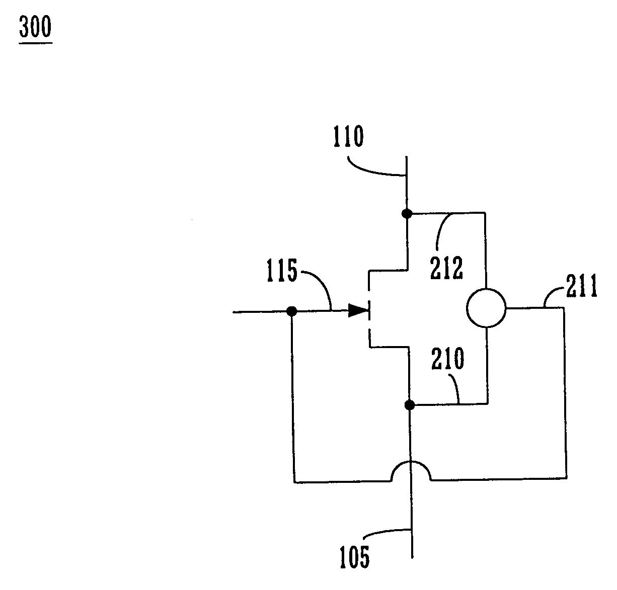
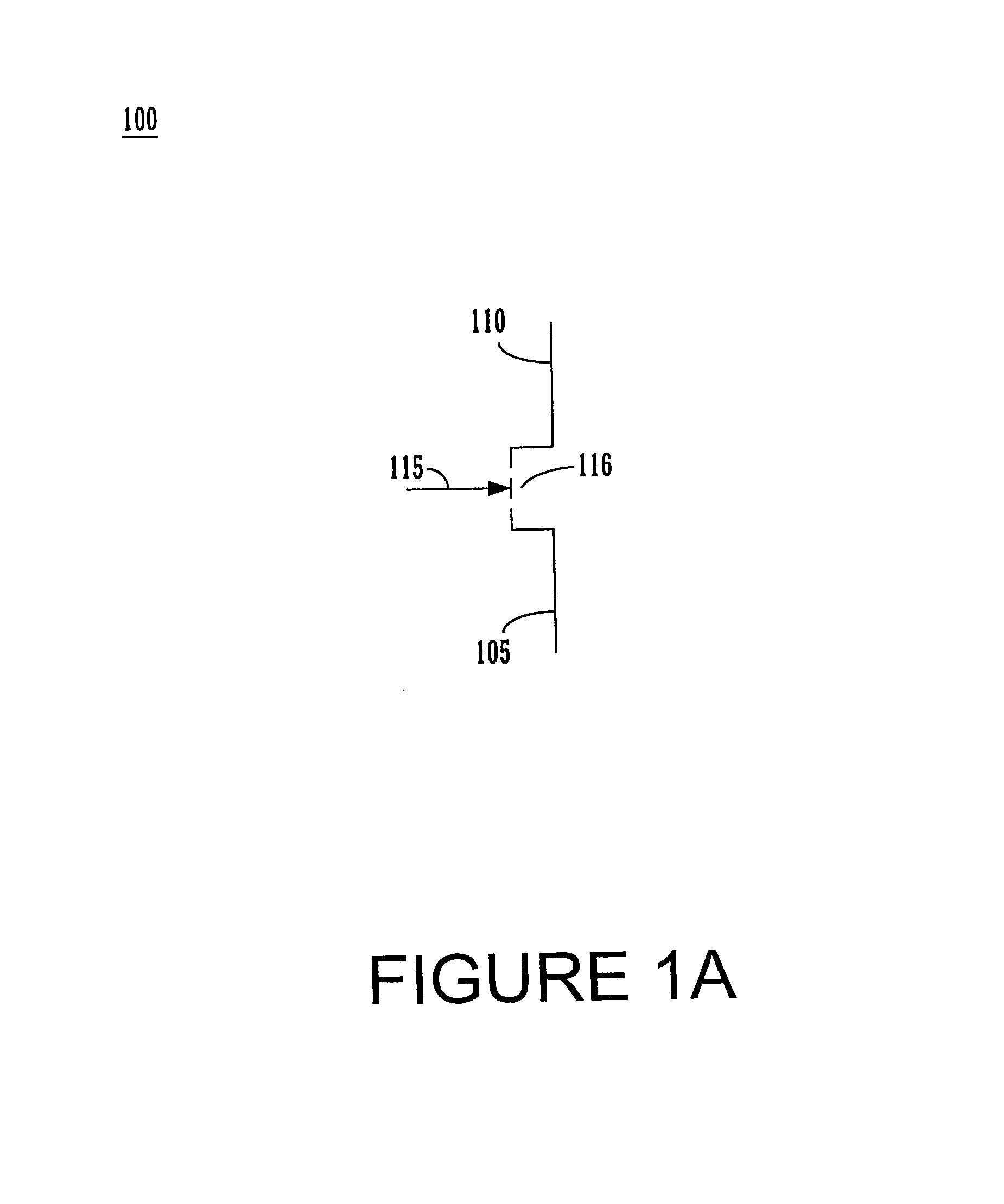
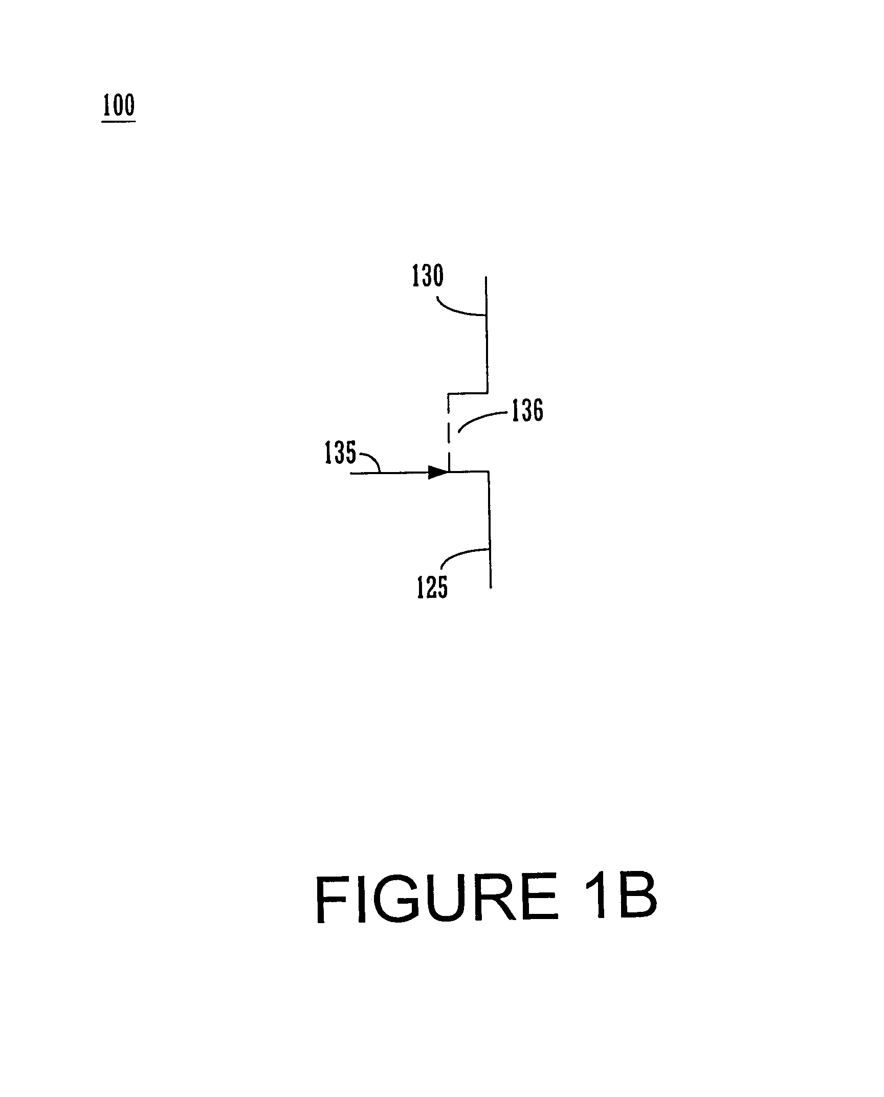
[0029]FIG. 1 shows the electronic symbols used in the present invention to represent three different normally off FETs 100. FIG. 1a is the electronic symbol used to represent an n-channel, symmetrical, normally off JFET. The gate lead 115 is spaced equidistant between the source lead 105 and the drain lead 110 which identifies this as a symmetrical device. The direction of the arrow on the gate lead signifies an n-channel JFET. The broken line 116 between source and dr...


PUM


Abstract

A semiconductor switching device or amplifier combined in parallel with one or more active devices defined as starter devices. A starter device is used to reduce the terminal voltage of a switching device or amplifier to a dc level below about 0.4 volts which will then allow the switching device to easily change between the on or conducting state and the off or non-conducting state. Three different starter devices are utilized. The first being a Bipolar Junction Transistor (BJT), the second a Metal Oxide Silicon Field Effect Transistor (MOSFET), and the third consisting of three normally off JFETs connected serially. Generally, a single starter device is coupled across the terminals of a semiconductor switching device or amplifier, but it is possible and sometimes advantageous to couple two or more starter devices in parallel. In a first case, a symmetrical, normally off or enhancement mode JFET is used as the switch or amplifier. A starter device coupled between source and drain of the JFET will allow operation at dc voltage levels above 0.4 volts. In a second case, an asymmetrical, normally off JFET is used as the switch or amplifier. A starter device coupled between source and drain of the JFET will allow operation at dc voltage levels above 0.4 volts. In a third case, a normally off MESFET is used as the switch or amplifier. A starter device coupled between source and drain of the MESFET will allow operation at dc voltage levels above 0.4 volts.

Description

CROSS-REFERENCE TO RELATED APPLICATIONS[0001]This is a continuation of patent application Ser. No. 09 / 708,336, filed Nov. 7, 2000, now of U.S. Pat. No. 6,614,289 issued Sep. 2, 2003.RELATED APPLICATIONS[0002]The following copending U.S. patent application Ser. No. 09 / 430,500, “NOVEL JFET STRUCTURE AND MANUFACTURE METHOD FOR LOW ON RESISTANCE AND LOW VOLTAGE APPLICATIONS”, Ho-Yuan Yu, filed 2 Dec., 1999, is incorporated herein by reference for all purposes. The following copending U.S. provisional patent application Ser. No. 60 / 167,959, “STARTER DEVICE FOR NORMALLY “OFF” JFETS”, Ho-Yuan Yu, filed 29 Nov., 1999, is incorporated herein by reference for all purposes.BACKGROUND OF THE INVENTION[0003]1. Field of the Invention[0004]The present invention relates generally to the field of active semiconductor devices. More specifically, the present invention relates to novel semiconductor device structures useful in low voltage and high current density applications. More particularly, the pr...

Claims


Application Information

Patent Timeline
Patent Type & Authority Patents(United States)
IPC IPC(8): H01L27/098H03K17/041H03K17/0416H03K17/06H03K17/567
CPCH01L27/098H03K17/04106H03K17/04163H03K17/063H03K17/567
Inventor YU, HO-YUAN
Owner POWER INTEGRATIONS INC
Why Eureka
Try Eureka