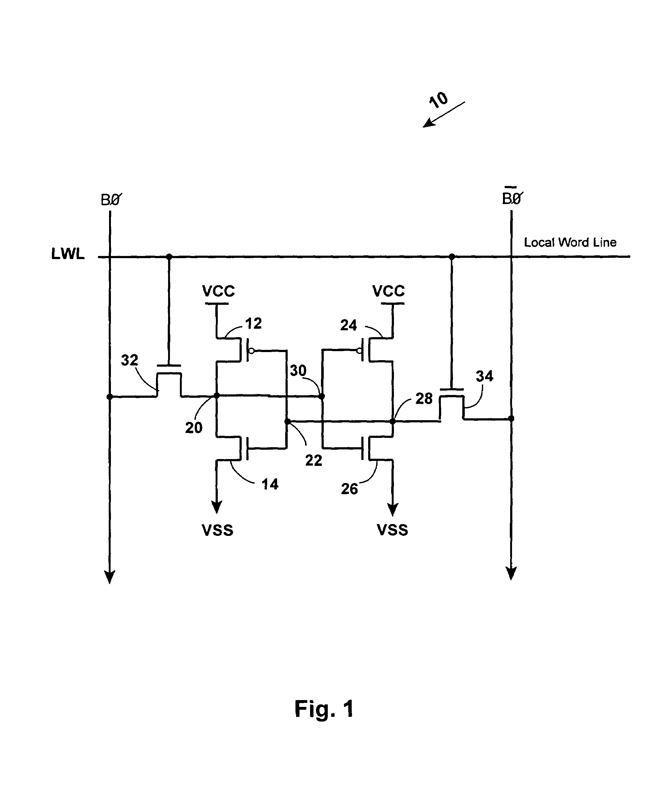
[0024]The present invention provides a SRAM having an internal data bus with reduced internal
signal levels to save power in a read mode of operation. The SRAM has a plurality of banks of memory cells, with each
bank of memory cells having a memory-
cell core in which the memory cells are arranged in word rows and bit columns. Each
memory cell in a
bank receives a local word line
signal for selecting a row of memory cells and for connecting a selected
memory cell of a particular column to a respective bit-
line pair to provide a low-voltage differential voltage read-output signal from that
memory cell to a bit-
line pair for its respective bit column. A Y-
multiplexer directly connects each bit-
line pair of a respective column to one end of a corresponding pair of differential data bitlines of an internal data bus while substantially maintaining the
low voltage differential voltage level signals on the pairs of differential data bitlines of the internal data bus. Differential
sense amplifier / output buffers are each connected to the other end of a respective pair of differential data bitlines in an internal data bus. Each of the
sense amplifier / output buffers receives a
low voltage differential voltage level signal from a corresponding bit-line pair and each of the
sense amplifier / output buffers has output signals that are full VDD / VSS logic-level signals. Adjacent to each of a plurality of SRAM data output terminals are located corresponding differential sense
amplifier / output buffers that provides full
logic level signals to that SRAM data output terminal. The internal data bus is a differential data bus that carries
low voltage differential voltage level signals that are not full logic levels from memory cells to the differential sense
amplifier / output buffers to thereby reduce power consumed by not driving full
logic level signals through the internal data bus.
[0026]The capacitances of the bit-line pairs in each core of a
memory bank are approximately the same as the capacitances of the internal data bus for all of the memory banks to minimize the total capacitance of the lines from the memory
cell to the corresponding output terminals.
[0028]The present invention also provides a method of routing signals through a SRAM. The method includes the steps of: arranging a plurality of banks of memory cells in rows and columns, with each
bank of memory cells having a core in which the memory cells are arranged in word rows and bit columns, each memory cell in a bank receiving a local word line signal for selecting a row of memory cells and for connecting the memory cells of a column to a respective bit-line pair to provide a
LOW VOLTAGE differential voltage signal from a memory cell to a bit-line pair for a respective bit column; directly connecting each bit-line pair of a respective columns through a Y-
multiplexer circuit to one end of a corresponding pair of differential data bitlines in an internal data bus while substantially maintaining low voltage differential voltage level signals on the pairs of differential data bitlines of the internal data bus; connecting differential sense
amplifier / output buffers to the other end of a respective pair of differential data bitlines in an internal data bus, each of said sense amplifier / output buffers receiving low voltage differential voltage level signals from a corresponding bit-line pair, and each of said sense amplifier / output buffers having output signals that are full
logic level signals; locating corresponding differential sense amplifier / output buffers adjacent to one of a plurality of SRAM data output terminals, each of which buffers provides full logic level signals to that SRAM data output terminal. The method provides that the differential data bus carries low voltage differential voltage level signals that are not full logic levels from memory cells to the differential sense amplifier / output buffers to thereby reduce power consumed by not driving full logic level signals through the internal data bus.
[0029]The method also includes forming bit-line pairs in a memory core as twisted pairs and as adjacent twisted pairs in lower
metal layers of the SRAM, with horizontal twists. The method includes forming lines of the differential data bitlines in the internal data bus as twisted pairs and as adjacent twisted pairs in upper metal layers of the SRAM, with
horizontal and vertical twists. The method further includes forming the capacitance of the bit-line pairs in each core of a
memory bank to be approximately the same as the capacitance of the internal data bus for all of the memory banks to minimize the total capacitance of the lines from a memory cell to an output terminal.

