Image forming apparatus

a technology of image forming apparatus and magnet brush, which is applied in the field of printers, can solve the problems of unsolved, degrade reproducibility and therefore tonality, and the magnet brush therefore fails to uniformly contact the photoconductive element, so as to and reduce the half width of the main magnetic pol

Inactive Publication Date: 2005-12-20
RICOH KK
View PDF3 Cites 20 Cited by
  • Summary
  • Abstract
  • Description
  • Claims
  • Application Information

AI Technical Summary

Benefits of technology

[0031]It is a first object of the present invention to provide an image forming apparatus capable of obviating the thinning of a horizontal line and the omission of a trailing edge and causing a minimum of background fog to occur, and a developing device therefore.
[0032]It is a second object of the present invention to provide an image forming apparatus capable of obviating the thinning of a horizontal line and the omission of a trailing edge, enhancing a developing ability, and causing a minimum of carrier from flying about, and a developing device therefor.
[0033]It is a third object of the present invention to provide an image forming apparatus capable not only of obviating the thinning of a horizontal line and the omission of a trailing edge but also of reducing granularity, and a developing device therefor.

Problems solved by technology

The two-ingredient type developer, however, brings about the following problems.
The method taught in the document, however, has the following problems left unsolved.
The magnet brush therefore fails to uniformly contact the photoconductive element.
This degrades the reproducibility and therefore tonality of a so-called high contrast portion.
Should the amount of charge to deposit on the toner be reduced to avoid the deposition of the carrier, uncharged toner would increase and contaminate the background of an image.
However, an electric field for development available with non-contact type development using the two-ingredient type developer is too weak to enhance a developing ability.
In the conventional developing device, the above defects can be reduced to an acceptable level if the background potential is reduced to, e.g., about 100 V or about 50 V. Such a low background potential, however, brings about background contamination or fog.
However, a problem with this apparatus is that the magnet brush actively moves in a small gap between an image carrier and a developer carrier, causing the carrier to fly about during development and deposit on the image carrier as well as on the other members.
The carrier therefore prevents toner around the carrier from being transferred to a paper sheet or similar recording medium, resulting in a defective image.
Moreover, if the carrier is transferred to the paper sheet, it simply constitutes an impurity in the resulting image because it is not fixed on the paper sheet.
Granularity is one of major causes that lower image quality.
This wastefully consumes toner and needs replenishment of extra toner while increasing the amount of waste toner collected.
The toner deposited on such members is transferred to the back or the background of the resulting print, making the print defective.
Moreover, the toner forming the patch flies about to contaminate the density sensor.
The toner deposited on the sensor lowers the output of the sensor and thereby obstructs the accurate sensing of density.
This method, however, is not a drastic solution because it needs the extra means and requires the operator or a serviceman to clean the sensor.
In addition, the patch size should be as small as possible because the contamination derived from the path lowers sensing accuracy.
It is therefore difficult to improve both of a high density portion and a low density portion at the same time.
It is generally considered to be difficult to achieve an attractive image by satisfying the two conditions over the entire density range.
However, a greater development gap enhances an edge effect during development, i.e., develops solitary dots in a greater size than expected, thickens lines, enhances a portion around a solid image portion or a halftone image portion or causes the outside of such an image portion to be lost.
A small development gap, however, intensifies the frictional force of the magnet brush and thereby aggravates the omission of a trailing edge and that of dots while obstructing the reproduction of a horizontal line.
A problem in this respect is that high pixel density reduces the individual pixel relative to the spot diameter of a beam to issue from an exposing unit, preventing sufficient tonality from being achieved.
This is because when a solitary dot is written, a latent image representative of it is shallow due to low exposure energy density, making reproduction unstable.
On the other hand, in a high density portion, nearby pixels are exposed in such a manner as to overlap each other with the result that image density rapidly saturates relative to a density area ratio, causing gamma to rise, i.e., lowering tonality.
Today, high resolution and high tonality, which have been difficult to achieve with conventional image forming apparatuses due to accuracy and cost problems, are available with may products.
However, as for exposure using a beam whose spot diameter is equivalent to a pixel size, tonality is not sufficient when it comes to recent, high density images.
This aggravates irregularity in the area of the dot and thereby lowers the reproducibility of a highlight portion.
Moreover, when the recording density is as high as 1,200 dpi, solitary dots are further reduced in size and cannot be easily formed by development.

Method used


Image

  • Image forming apparatus
  • Image forming apparatus
  • Image forming apparatus

Examples


first embodiment

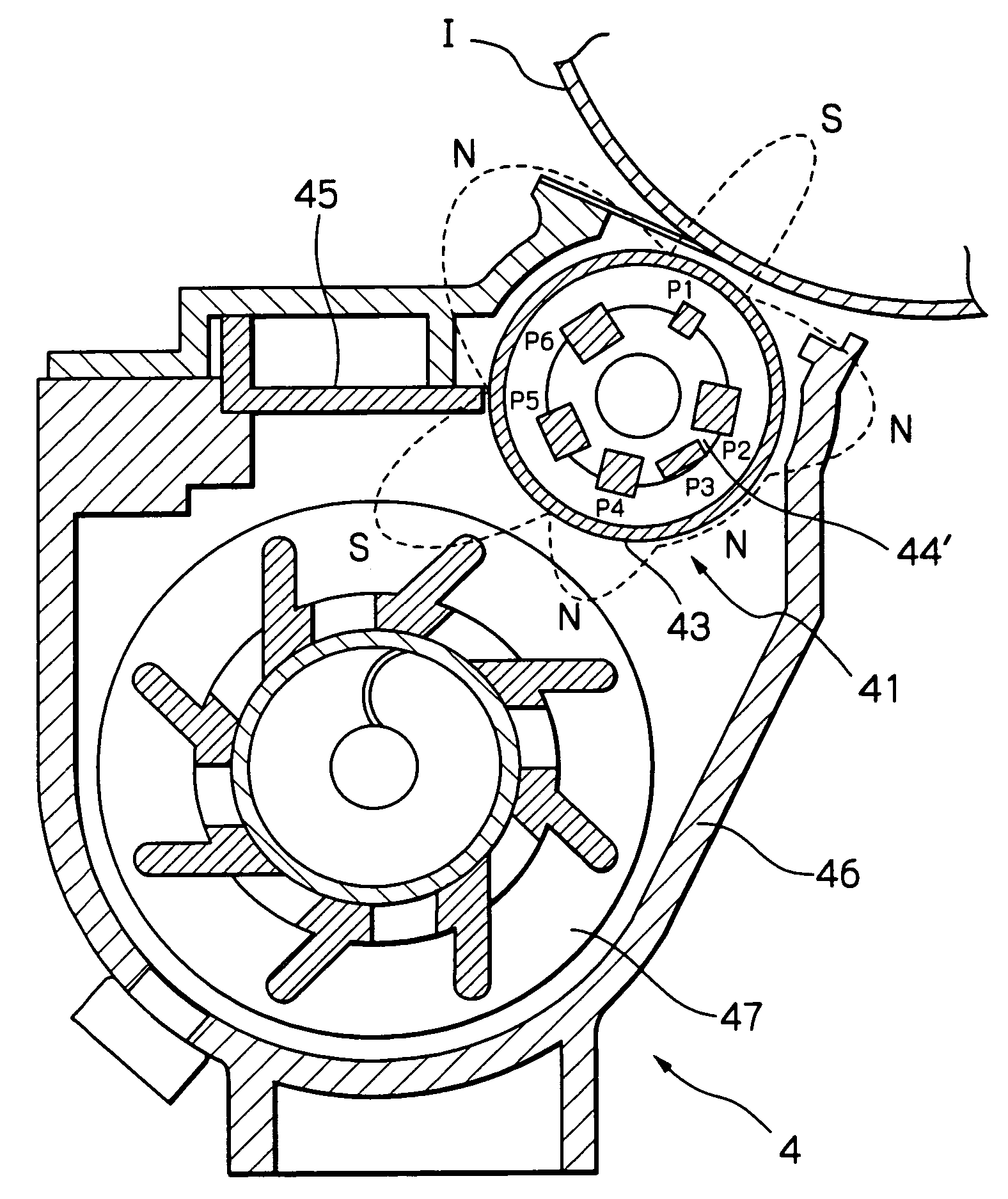
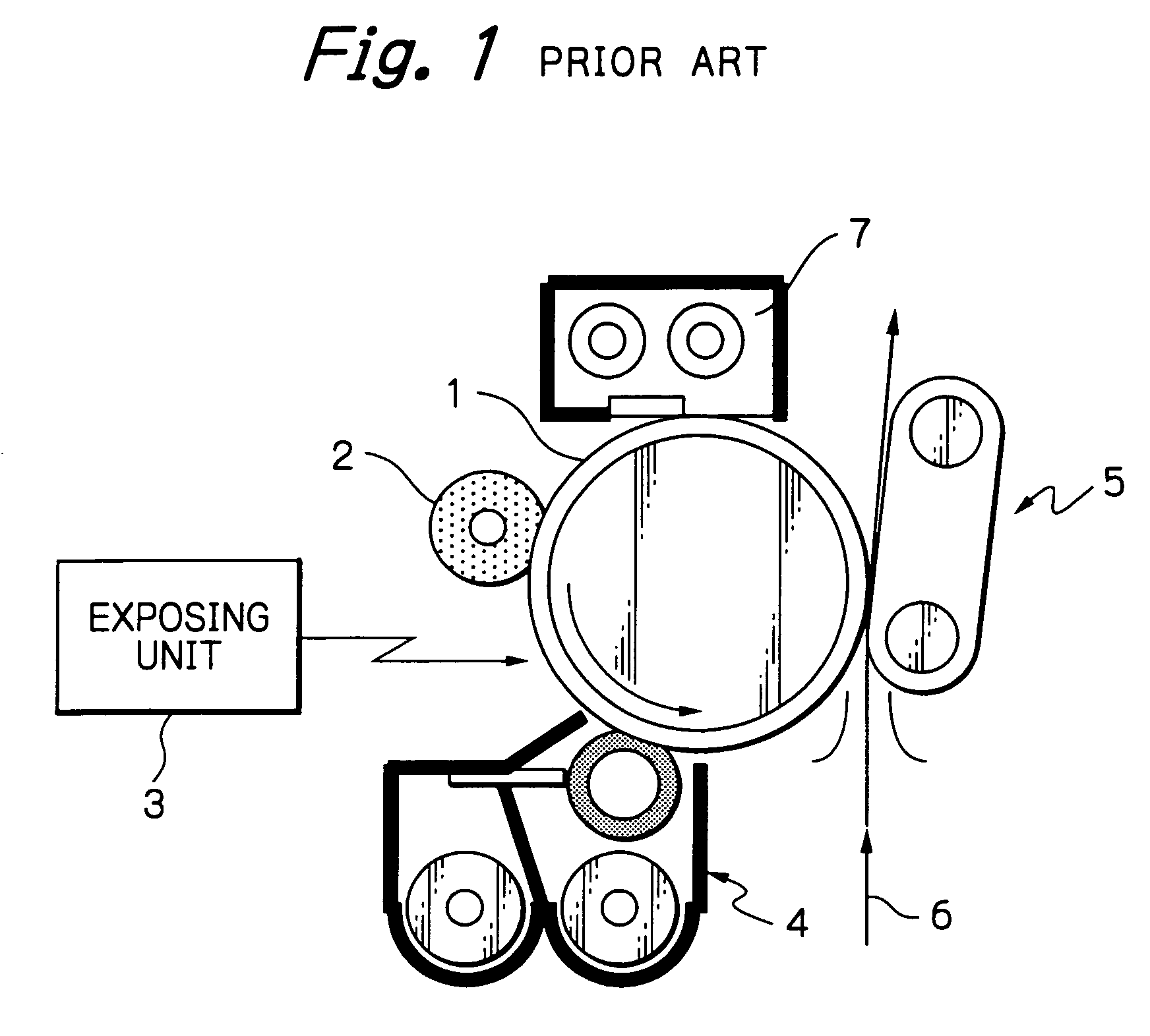
[0102]This embodiment is mainly directed toward the first object stated earlier. The illustrative embodiment is essentially identical with the image forming apparatus described with reference to FIGS. 1 and 2 as to the general mechanical structure. The structure of FIGS. 1 and 2 will be described more specifically. In FIG. 1, the drum 1 is implemented by, e.g., a conductor coated with a photoconductive material and is rotatable at a peripheral speed of, e.g., 230 mm / sec. The charger 2 includes a roller contacting the drum 1 and a power supply for applying a voltage to the roller. The charger 2 uniformly charges the surface of the drum 1 to a preselected potential, e.g., −0.6 kV. The exposing unit 3 includes a light source, e.g., a laser diode for emitting a laser beam. The laser beam scans the charged surface of the drum 1 in accordance with image data to thereby form a latent image on the drum 1.

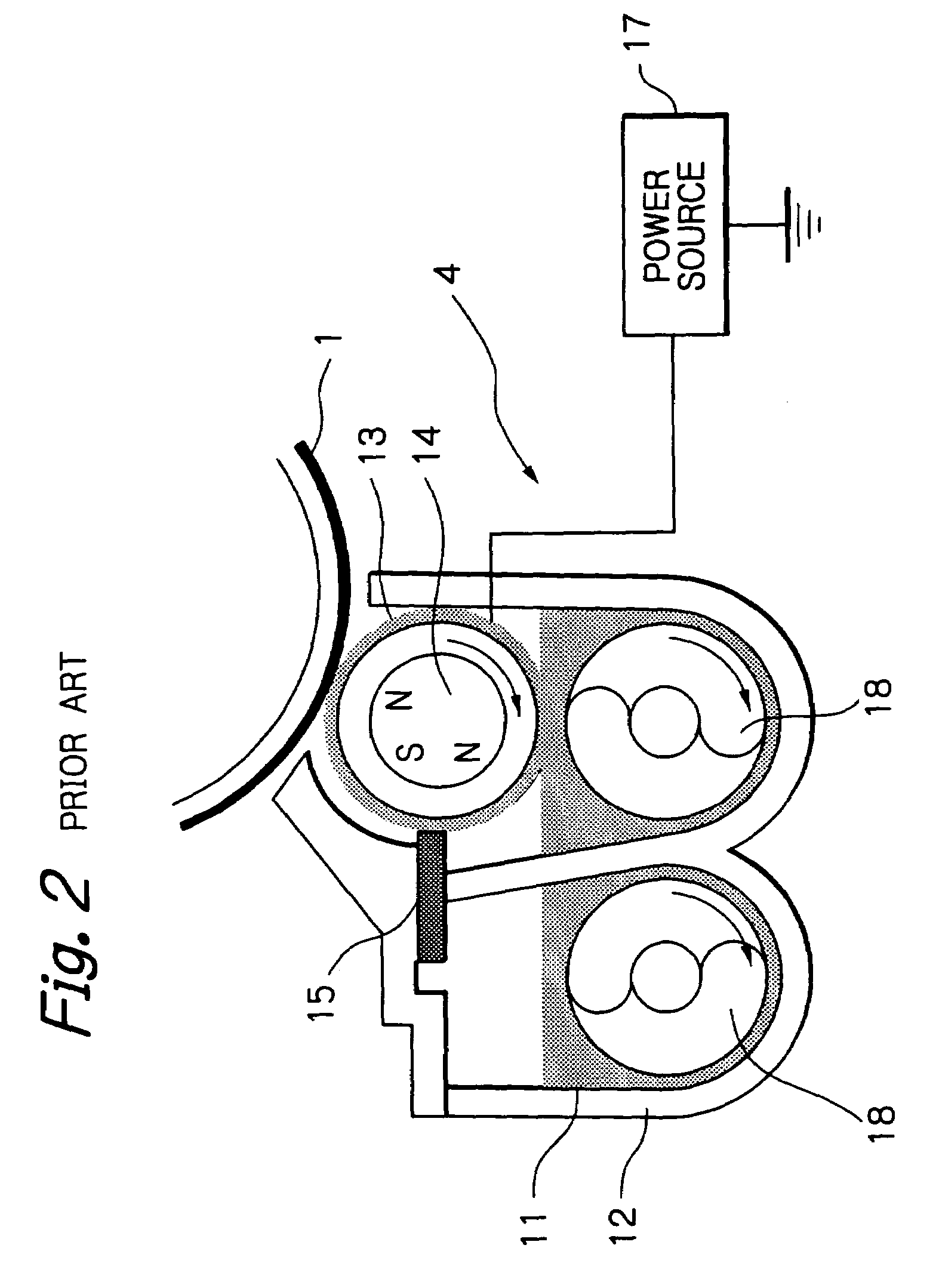
[0103]The developing device 4 develops the latent image with toner for thereby forming ...

second embodiment

[0121]This embodiment is identical with the first embodiment except for the additional condition that the charge potential is 1,000 V or below in absolute value.

[0122]Generally, a field strength that insures insulation of OPC (Organic PhotoConductor) often used for an electrophotographic apparatus is between 30 V / μm and 40 V / μm. If the field strength exceeds such a range, then OPC itself looses its function (insulation) or has its life shortened in a long term.

[0123]FIG. 7 shows the results of image estimation conducted by passing 10,000 paper sheets and varying the potential to deposit on a photoconductive element over the range of from 200 V to 1,200 V. The photoconductive element was implemented by OPC and made up of a co-called CTL (Charge Transport Layer) and a CGL (Charge Generating Layer) that were 27 μm thick and 1 μm thick, respectively. A color copier imagio MF4570 available from Ricoh Co., Ltd. was used to print a test chart whose image area ratio was 5%.

[0124]As shown in...

third embodiment

[0125]This embodiment is identical with the first embodiment except for the additional condition that the charge potential is 100 V or below in absolute value.

[0126]FIG. 8 lists the density of black solid images measured by using a developer whose toner was charged to 10 μC / g to 35 μC / g and by varying the bias for development. As FIG. 8 indicates, when the amount of charge to deposit on toner is 10 μC / g to 35 μC / g that reduces both of background contamination and the thinning of a horizontal line omission of a trailing edge, a bias of 100 V or above is necessary for the image density of 1.3 or above to be attained.

[0127]Further, in electrophotographic image forming apparatuses in general, the charge potential and bias for development vary by 20 V to 30 V. Specifically, the charge potential varies due to the wear, i.e., variation in the film thickness of a photoconductive element ascribable to aging and due to the varying environment, particularly humidity. The bias for development v...


PUM


Abstract

An electrophotographic image forming apparatus of the present invention frees images from various defects including the thinning of horizontal lines, the omission of the trailing edge of an image, background contamination, granularity particular to a halftone image, carrier scattering, and image noise. Further, the apparatus of the present invention solves problems ascribable to patches used to sense image density. Moreover, the apparatus of the present invention faithfully reproduces tonality and has a high developing ability.

Description

CROSS-REFERENCE TO RELATED DOCUMENTS[0001]The present application is a divisional of U.S. application Ser. No. 09 / 846,244 filed on May 2, 2001 now U.S. Pat. No. 6,757,509, and in turn claims priority to JP 2000-133628 filed on May 2, 2000, JP 2000-133629 filed on May 2, 2000, JP 2000-142342 filed on May 15, 2000, JP 2000-142344 filed on May 15, 2000, JP 2000-178923 filed on Jun. 14, 2000, JP 2000-183567 filed on Jun. 19, 2000, and JP 2000-205494 filed on Jul. 6, 2000, the entire contents of each of which are hereby incorporated herein by reference.BACKGROUND OF THE INVENTION[0002]The present invention relates to a printer, digital copier, facsimile apparatus or similar electrophotographic image forming apparatus. More particularly, the present invention relates to a developing method for causing a developer to form a magnet brush on a developer carrier in a developing region for developing a latent image formed on an image carrier, and a device for practicing the same.[0003]A develo...

Claims


Application Information

Patent Timeline
Patent Type & Authority Patents(United States)
IPC IPC(8): G03G9/10G03G13/09
CPCG03G9/10G03G13/09G03G2215/0119G03G2215/0177
Inventor SHOJI, HISASHIKAI, TSUKURUYASUTOMI, KEIMATSUURA, NEKKATAKEUCHI, NOBUTAKASUZUKI, HIROKATSU
Owner RICOH KK
Why Eureka
Try Eureka