Semiconductor device and method for manufacturing the same

a semiconductor and semiconductor technology, applied in the direction of semiconductor devices, electrical equipment, transistors, etc., can solve the problems of low mobility of electric field effect transistors, inability to operate at the frequency necessary for processing picture signals, and system in which a driver ic is mounted, etc., to achieve high numerical aperture

Inactive Publication Date: 2006-01-03
SEMICON ENERGY LAB CO LTD
View PDF48 Cites 28 Cited by
  • Summary
  • Abstract
  • Description
  • Claims
  • Application Information

AI Technical Summary

Benefits of technology

[0015]An object of the present invention is to make the arrangement of pixel electrodes, scanning lines (gate lines) and data lines formed in a pixel section appropriate, and provide a pixel construction wherein a high numerical aperture is realized without increasing the number of masks nor the number of steps.
[0016]Furthermore, an object thereof is to provide a technique for improving properties of a TFT, and realizing the construction of the TFT optimal for conditions for driving a pixel section or a driving circuit, using a fewer photo masks.
[0023]By putting the semiconductor film between the first electrode and the second electrode and applying the same voltage thereto, substantially the same effect as obtained by making the film thickness of the semiconductor film substantially half can be obtained. Moreover, a depletion layer is rapidly spread so that the sub-threshold coefficient can be made small. The electric field effect mobility can be improved. Particularly by making edges of the first electrode and the second electrode consistent with each other in the cross portion of the electrodes and the semiconductor film, the advantageous effect can be more satisfactorily exhibited.
[0024]By making the first interconnection and the second interconnection up to a data line and a scanning line, respectively, a pixel section corresponding to an active matrix driving system can be formed. By combining the first and fourth insulating films, pixel electrodes can be formed as a topmost layer. By forming the interconnections to overlap with each other, the area thereof can be made large. By such a construction, the numerical aperture of pixels can be improved.

Problems solved by technology

However, TFTs have a low electric field effect mobility and cannot be operated by frequencies necessary for processing picture signals.
However, as the density of pixels becomes larger, the pitch of the pixels becomes narrower; therefore, it is considered that the system in which a driver IC is mounted has a limit.
An increase in the number of the connecting terminals causes an increase in the probability that contact faults are generated.
As a result, it is unsuccessful that a semiconductor device using this as a display is made small-sized, and the design of the appearance thereof is damaged.
However, even if polycrystal silicon is used to form TFTs, after all the electric properties thereof are not equivalent to the properties of MOS transistors formed in a monocrystal silicon substrate.
This method has a problem that off-state current is large because of defects formed in boundaries between crystal grains.
However, if the number of the photo masks is simply increased in order to make the construction of the TFTs optimal in accordance with requests for a pixel section or respective driving circuits, the manufacturing steps become complicated and the number of the steps increases unavoidably.

Method used


Image

  • Semiconductor device and method for manufacturing the same
  • Semiconductor device and method for manufacturing the same
  • Semiconductor device and method for manufacturing the same

Examples


example 1

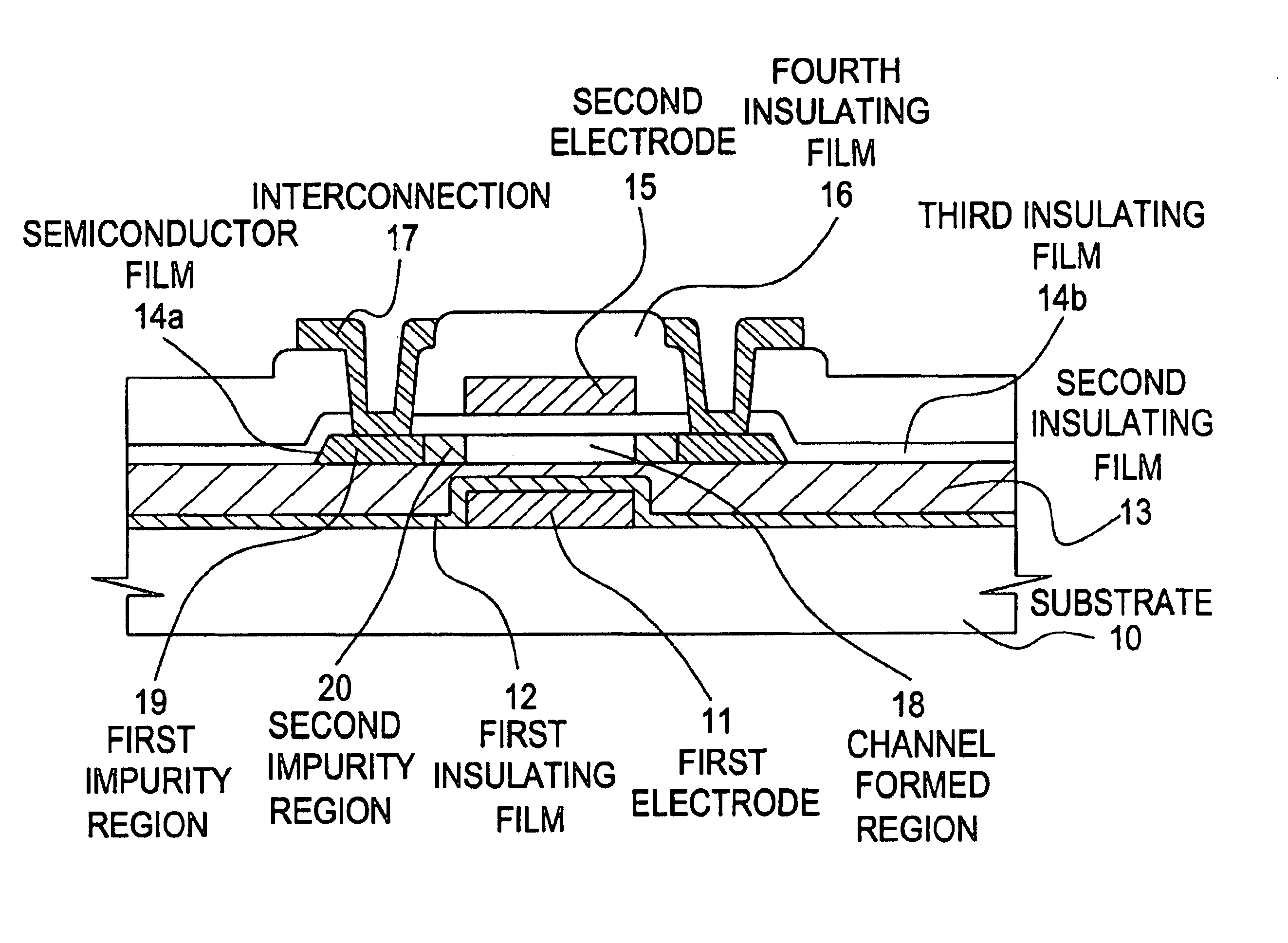
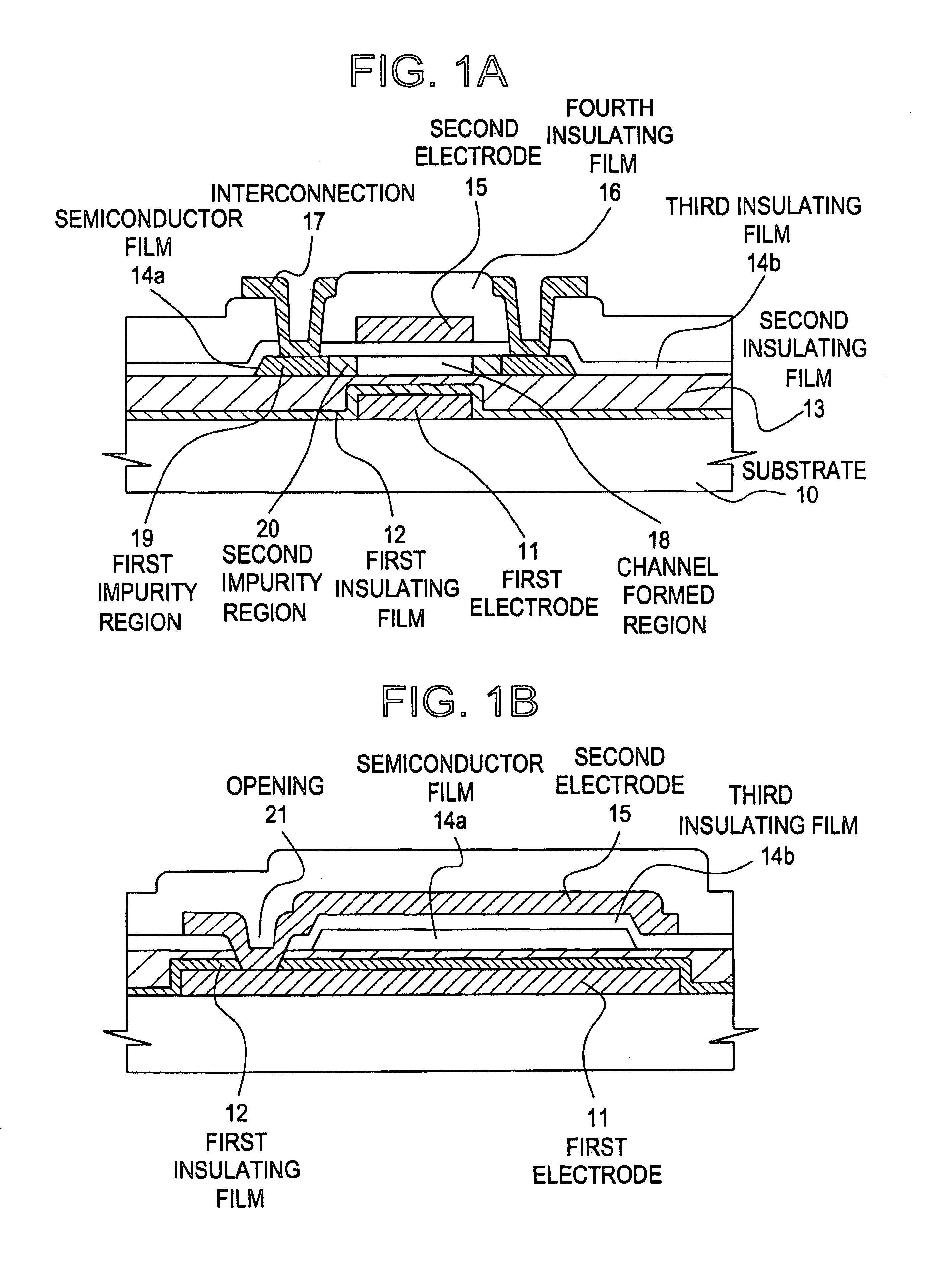
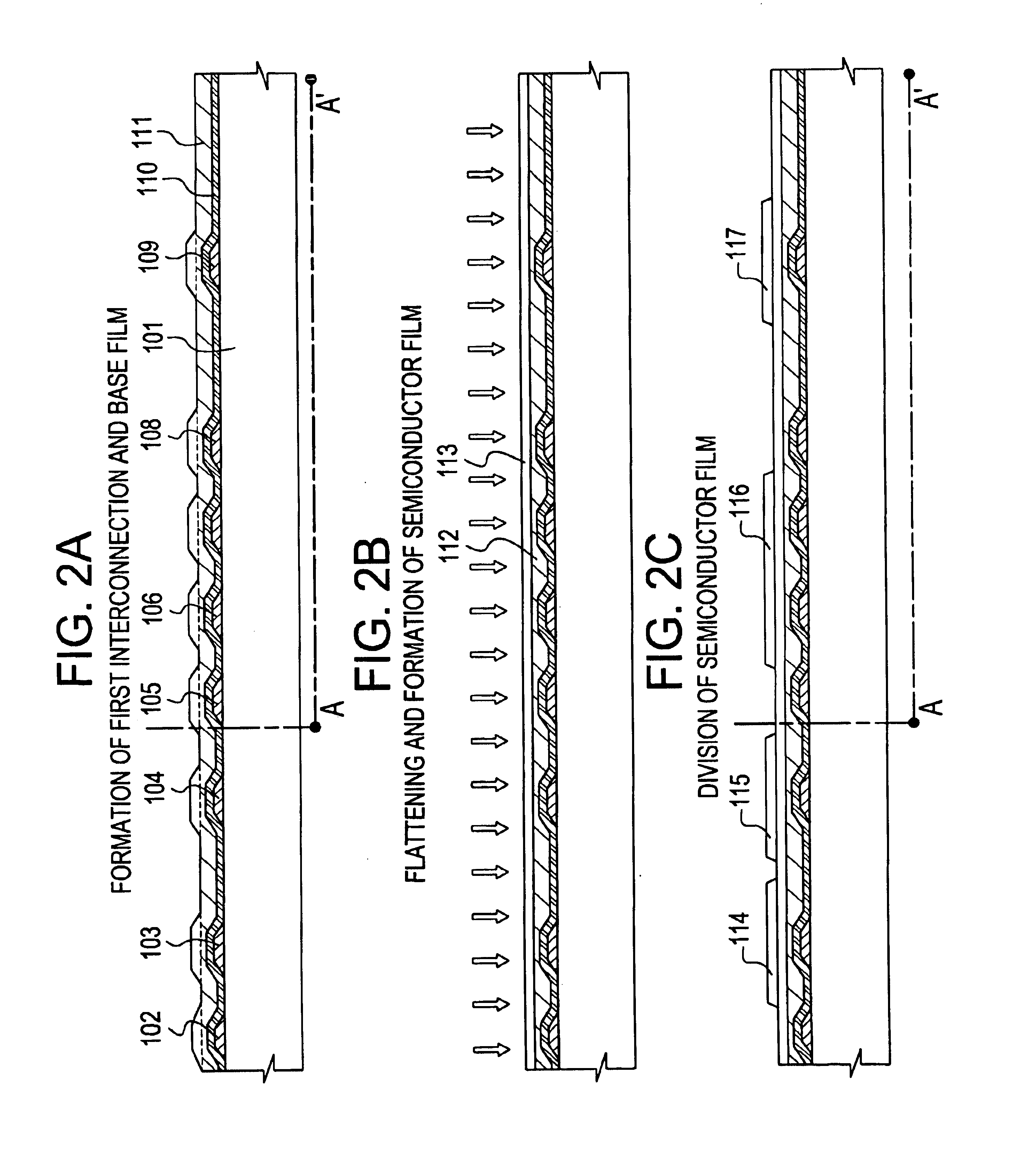
[0056]Referring to the drawings, an embodiment of the present invention will be described. Herein, there will be detailed a process of forming a pixel section and TFTs (n-channel type TFTs and p-channel type TFTs) of a driving circuit set up near the pixel section, simultaneously, on the same substrate. FIGS. 2 to 6, which are referred to in the present embodiment, are sectional views for explaining the steps of manufacturing them. FIGS. 7 to 9 are top views corresponding thereto. For convenience of the description, common reference numbers are used.

[0057]In FIG. 2A, for a substrate 101, a glass substrate, a quartz substrate, a ceramic substrate or the like can be used. It is allowable to use an insulating film formed on the surface of a silicon substrate, a metal substrate or a stainless substrate. It is also allowable to use a heat-resistant plastic substrate giving resistance against treating temperature in the present example.

[0058]First interconnections 102, 105 and 108 and fir...

example 2

[0090]Another embodiment of the present invention will be described, referring to drawings. One example of the construction of a pixel construction and a driving circuit suitable for a liquid crystal display device will be described. FIGS. 10 and 11, which are referred to in the present embodiment, are sectional views for explaining the process of the manufacture thereof. FIGS. 12 and 13 are top views corresponding thereto. In the following description, common reference numbers are used for convenience.

[0091]In FIG. 10A, a substrate 301, first interconnections 302 to 306, and semiconductor films 310 to 312 divided into an island form are the same as in Embodiment 1. FIG. 12A illustrates atop view thereof in this state.

[0092]First, a first insulating film 307 of a silicon oxynitride film is formed to have a thickness of 50 nm. A silicon oxide film made by TEOS is used to form a second insulating film 308 of 1 μm thickness. The surface is made flat by CMP, and subsequently a silicon o...

example 3

[0106]FIG. 17 shows the characteristic of a 19-stage ring oscillator, which is an example of the operation characteristic of TFTs manufactured by the present invention. About the sizes of the TFTS, the channel length (L) and the channel width (W) of the n-channel type TFT are 5 μm and 10 μm, respectively, and the channel length (L) and the channel width (W) of the p-channel type TFT are 5 μm and 20 μm, respectively. The TFTs of the present invention are manufactured according to Example 1. First electrodes and second electrodes are formed along the up-and-down direction, to sandwich a semiconductor film to produce gate electrodes. Edges thereof are substantially aligned with each other.

[0107]Comparative sample 1 is composed of conventional TFTS, wherein first electrodes (gate electrodes) are formed on one side of a semiconductor film. Comparative sample 2 is a product wherein first electrodes and second electrodes are formed along the up-and-down direction to sandwich a semiconducto...


PUM


Abstract

A semiconductor device, comprises a first electrode, a semiconductor film, a first insulating film and a second insulating film formed between the semiconductor film and the first electrode, a second electrode, and a third insulating film formed between the semiconductor film and the second electrode. The semiconductor film is formed on a flat surface of the second insulating film. A cross portion where the first electrode and the second electrode cross the semiconductor film at the same position is formed. The first electrode and the second electrode are connected to each other through an opening made in the first insulating film and the second insulating film outside the cross portion.

Description

[0001]This application is a Continuation-In-Part of U.S. application Ser. No. 10 / 105,625 filed Mar. 26, 2002.BACKGROUND OF THE INVENTION[0002]1. Field of the Invention[0003]The present invention relates to a semiconductor device using a thin film transistor (hereinafter referred to as a TFT) wherein a semiconductor film formed on a substrate and having a crystal structure is used; and a process for manufacturing the same. The semiconductor device in the present specification means any device which functions by the use of a semiconductor characteristic, and the category of the semiconductor device manufactured by the present invention includes a display device, a typical example of which is a liquid crystal display device having therein TFTs, and a semiconductor integrated circuit (such as a microprocessor, a signal processing circuit, or a high frequency circuit).[0004]2. Description of Related Art[0005]In various semiconductor devices having therein semiconductor elements, such as ...

Claims


Application Information

Patent Timeline
Patent Type & Authority Patents(United States)
IPC IPC(8): H01L21/84H01L21/336H01L21/77H01L27/12H01L29/423H01L29/786
CPCH01L27/1214H01L29/42384H01L29/78648H01L29/78636H01L29/78645H01L29/6675H01L27/1248H01L27/1288
Inventor TSUNODA, AKIRAYAMAZAKI, SHUNPEIKOYAMA, JUN
Owner SEMICON ENERGY LAB CO LTD
Why Eureka
Try Eureka