

Data transmission system of directional coupling type using forward wave and reflection wave
- Summary
- Abstract
- Description
- Claims
- Application Information
AI Technical Summary
Benefits of technology
Problems solved by technology
Method used
Image

Examples
first embodiment
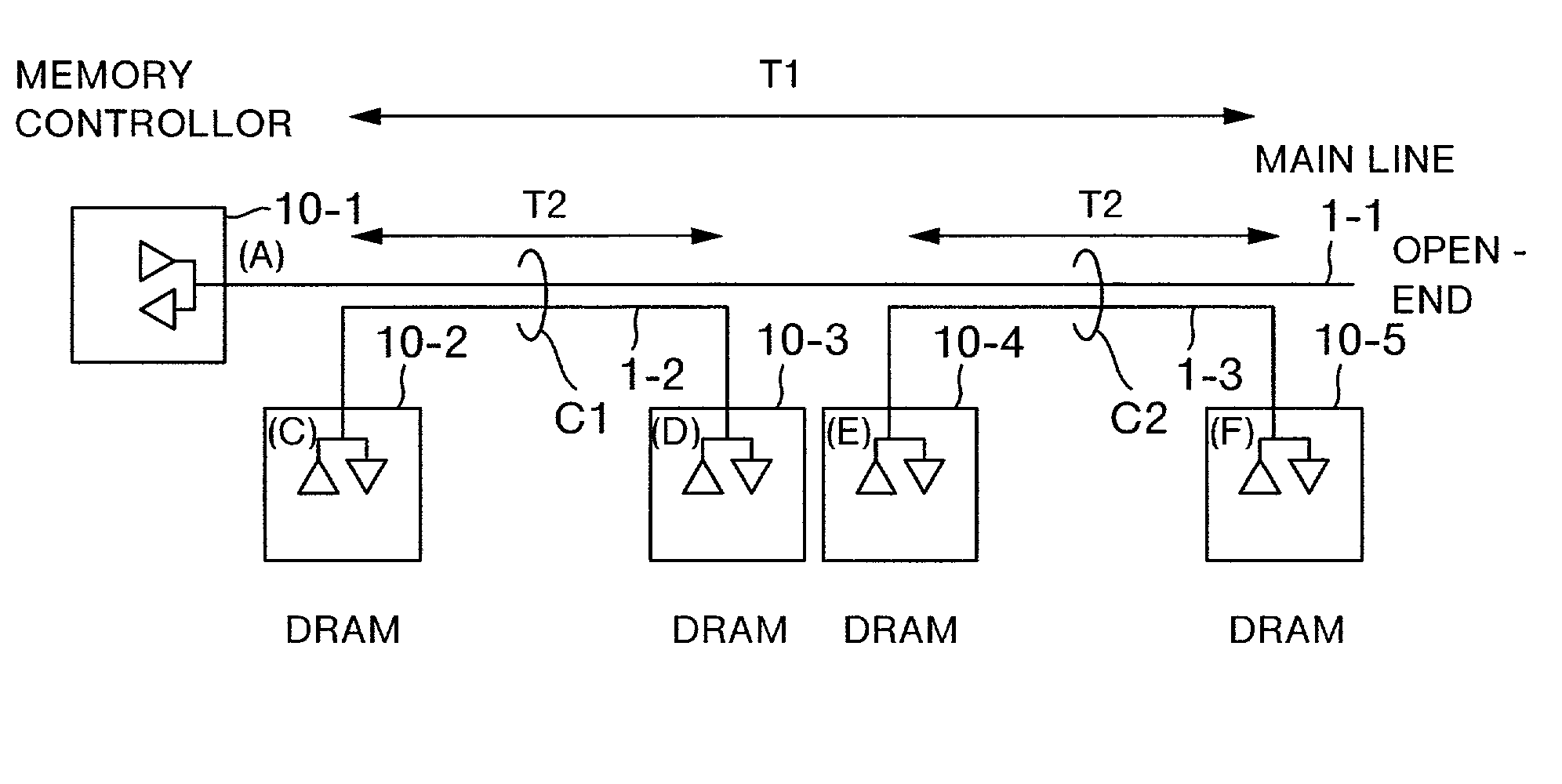
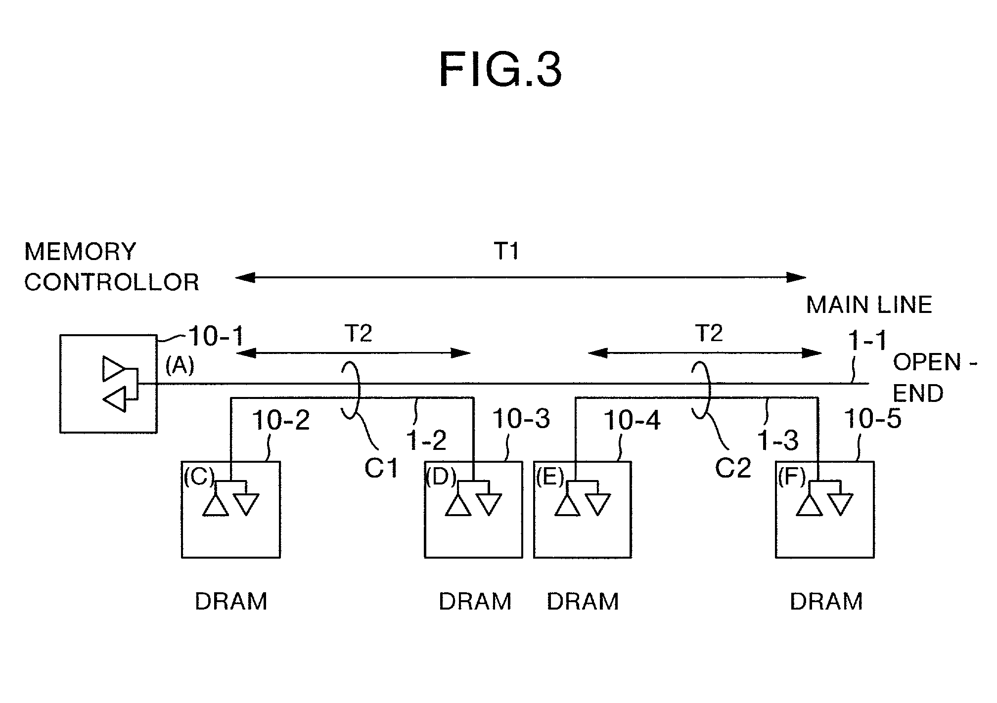
[0060]a bus system according to the invention will be described with reference to FIG. 1.
[0061]The bus system comprises an LSI chip 10-1 having a memory controller control mechanism (hereinafter simply referred to as a MC (memory controller) 10-1) and memory chips 10-2 to 10-5 (hereinafter simply referred to as DRAM's 10-2 to 10-5).
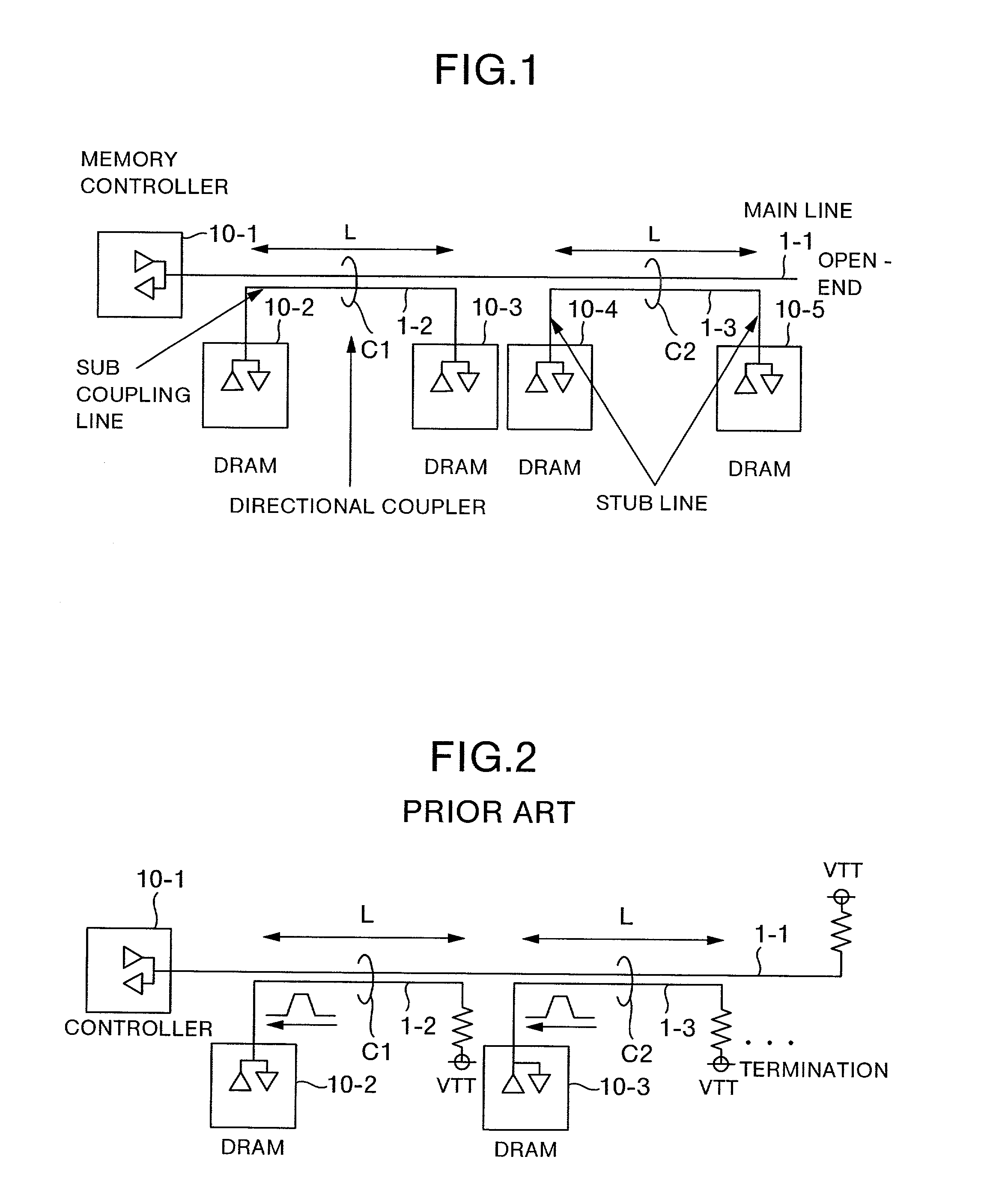
[0062]The MC 10-1 operates to read / write data from / to the DRAM's 10-2 to 10-5. Wiring lines 1—1 to 1-3 for read / write data transfer are provided, among which the line 1—1 connected to the MC 10-1 is especially called a main line. The line 1-2 includes three parts including a sub coupling line having a length of L and wired in parallel with the main line 1—1 to form a directional coupler and two stub lines led from both ends of the sub coupling line physically vertically thereof. In FIG. 1, the L-length sub coupling lines of lines 1-2 and 1-3 cooperate with the main line 1—1 to form directional couplers Cl and C2, respectively. Therefore, each of the direc...
PUM
 Abstract
Description
Claims
Application Information