Method and an apparatus of an inspection system using an electron beam

an inspection system and electron beam technology, applied in the direction of semiconductor/solid-state device testing/measurement, image enhancement, instruments, etc., can solve the problems of slow scanning speed, inability to locate the location of a defect on a wafer, and the time it takes to complete the processing steps becomes very long, so as to increase the speed of scanning a specimen

Inactive Publication Date: 2006-01-17
HITACHI LTD
View PDF39 Cites 9 Cited by
  • Summary
  • Abstract
  • Description
  • Claims
  • Application Information

AI Technical Summary

Benefits of technology

[0008]It is thus a first object of the present invention to provide an inspection method capable of increasing the speed of scanning a specimen using an electron beam and an inspection system adopting the method.
[0010]It is a third object of the present invention to provide an inspection method using an electron beam resulting in a small change in efficiency of detection of charged particles and an inspection system adopting the method.
[0018]According to still another preferred embodiment of the present invention, since charged particles are detected without passing through an objective lens, unlike the TTL system, even if a retarding voltage is reduced, the efficiency of detection of secondary electrons does not decrease and, in addition, the rotation of a picture can be made small.
[0020]According to a still further preferred embodiment of the present invention, an electron beam is put in a blanked state with a crossover of the electron beam serving as a fulcrum. If the electron beam is parallel beams with no crossover, the position of radiation of the blanked electron beam on a specimen changes, giving rise to a problem that an area adjacent to a radiation area is electrically charged inadvertently. In the case of this embodiment, however, since the electron beam is put in a blanked state with a crossover thereof serving as a fulcrum, the position of radiation of the electron beam on the specimen does not change, allowing the problem to be solved.

Problems solved by technology

However, while the ordinary SEM and the length measurement SEM are suited for observation of a limited field of vision at a high magnification, they are unsuitable for finding the location of a defect on a wafer.
It takes a very long time to search such an extremely large area by using an ordinary or length measurement SEM because the current of the electron beam thereof is small, resulting in a slow scanning speed.
As a result, if such SEMs are used in a process to fabricate a semiconductor device, the time it takes to complete the processing steps becomes very long, making the SEMs apparatuses of no practical use.
On the other hand, the TTL system brings about unnegligible problems such as a hindrance to the improvement of the scanning speed and a big rotation change of the electron beam accompanying a variation in specimen height, causing a resulting picture to rotate as well.
As shown by curve (2), the TTL system has a problem that, as the retarding voltage is reduced, the efficiency of detection of secondary electrons also decreases to such a small value that the problem caused by a low detection efficiency can not be ignored anymore.

Method used


Image

  • Method and an apparatus of an inspection system using an electron beam
  • Method and an apparatus of an inspection system using an electron beam
  • Method and an apparatus of an inspection system using an electron beam

Examples


Embodiment Construction

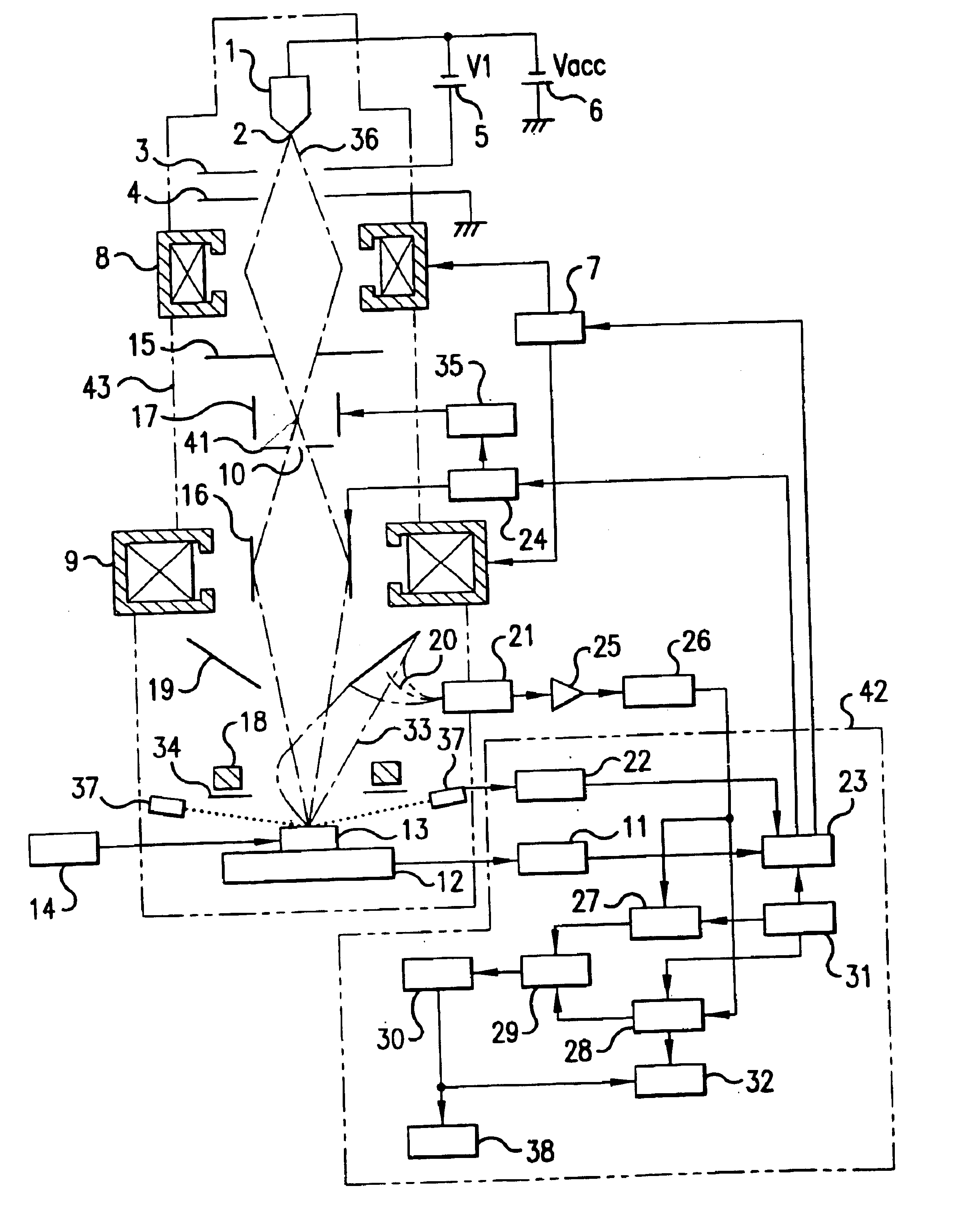
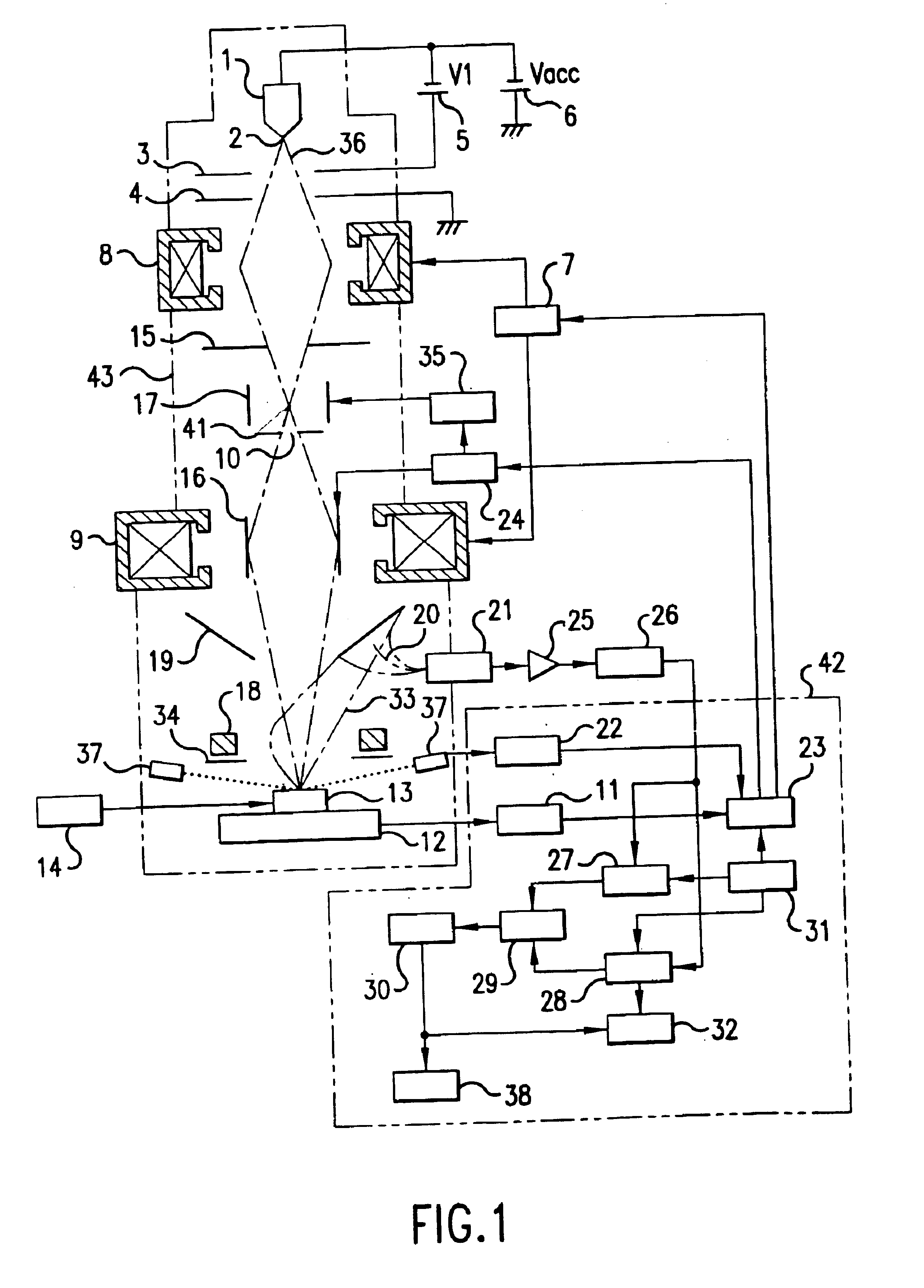
[0035]The present invention will become more apparent from a careful study of the following detailed description of a preferred embodiment with reference to the accompanying diagrams.

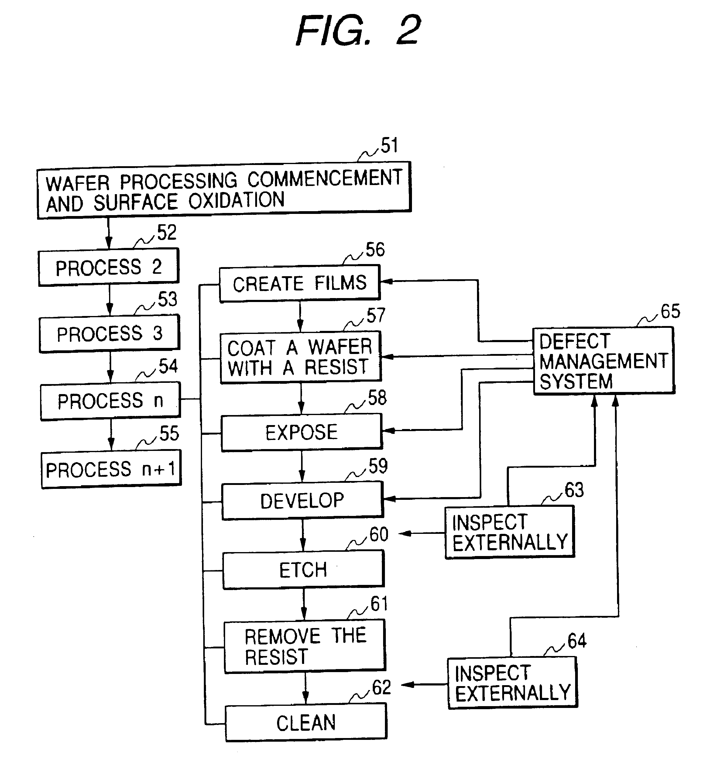
[0036]FIG. 2 is a block diagram showing a flow of a general process of fabricating a semiconductor device. As is obvious from the figure, in a process of fabricating semiconductor devices, steps 51 to 55 are repeated to create a number of patterns of semiconductor devices on wafers. Each of the steps to create a pattern comprises roughly a film creation step 56, a resist coating step 57, an exposure step 58, a development step 59, an etching step 60, a resist removing step 61 and a cleaning step 62. A circuit pattern will not be created normally on the wafer unless fabrication conditions are optimized at each of the steps.

[0037]External inspection steps 63 and 64 to inspect a circuit pattern are provided between the steps described above. When a defect is detected as a result of the inspections carried ...


PUM

PropertyMeasurementUnit
beam currentaaaaaaaaaa
energyaaaaaaaaaa
sizeaaaaaaaaaa

Abstract

Problems encountered in the conventional inspection method and the conventional apparatus adopting the method are solved by the present invention using an electron beam by providing a novel inspection method and an inspection apparatus adopting the novel method which are capable of increasing the speed to scan a specimen such as a semiconductor wafer.The inspection novel method provided by the present invention comprises the steps of: generating an electron beam; converging the generated electron beam on a specimen by using an objective lens; scanning the specimen by using the converged electron beam; continuously moving the specimen during scanning; detecting charged particles emanating from the specimen at a location between the specimen and the objective lens and converting the detected charged particles into an electrical signal; storing picture information conveyed by the electrical signal; comparing a picture with another by using the stored picture information; and detecting a defect of the specimen.

Description

[0001]This is a continuation of U.S. patent application Ser. No. 09 / 883,184, filed Jun. 19, 2001 which is a continuation of U.S. patent application Ser. No. 09 / 131,383, filed Aug. 7, 1998, which issued as U.S. Pat. No. 6,348,690 on Feb. 19, 2002.FIELD OF THE INVENTION[0002]In general, the present invention relates to an inspection method using an electron beam and an inspection apparatus adopting the method. More particularly, the present invention relates to an inspection method using an electron beam suitably for inspecting a pattern such as a circuit on a substrate in a process of fabricating a semiconductor device and an inspection apparatus adopting the method.BACKGROUND OF THE INVENTION[0003]There exists an apparatus for observing a specimen by using an electron beam which is known as a scanning electron microscope referred to hereafter simply as an SEM. In addition, as one of apparatuses for inspecting a semiconductor device, there is known a scanning electron microscope for ...

Claims


Application Information

Patent Timeline
Patent Type & Authority Patents(United States)
IPC IPC(8): H01J37/28G01Q30/02G01N23/00G01N23/20G01N23/225G21K1/08G21K7/00H01J37/22H01J37/244H01J37/256H01L21/66
CPCG01N23/20G03F7/7065G06T7/001H01J37/04H01J37/20H01J37/265H01J37/28G01N23/2251H01J2237/31766G06T2207/10056G06T2207/30148H01J2237/04756H01J2237/20221H01J2237/2444H01J2237/24592H01J2237/2817
Inventor IWABUCHI, YUKOTODOKORO, HIDEOMORI, HIROYOSHISATO, MITSUGUUSAMI, YASUTSUGUICHIHASHI, MIKIOFUKUHARA, SATORUSHINADA, HIROYUKIKANEKO, YUTAKASUGIYAMA, KATSUYATAKAFUJI, ATSUKOTOYAMA, HIROSHI
Owner HITACHI LTD
Why Eureka
Try Eureka