Stand-alone organic-based passive devices

a passive device and organic technology, applied in the direction of superconductor devices, waveguide types, waveguides, etc., can solve the problems of reducing the quality factor, adding to the complexity of modeling the device, and none of the above-mentioned inductor designs provides a suitable combination of low cost, high yield, and high current. , to achieve the effect of low cost, low cost and high performan

Inactive Publication Date: 2006-01-17
GEORGIA TECH RES CORP
View PDF93 Cites 57 Cited by
  • Summary
  • Abstract
  • Description
  • Claims
  • Application Information

AI Technical Summary

Benefits of technology

[0012]The present invention provides for low cost, and if desired high performance, discrete inductor devices in an all organic platform. The integrated passive devices (IPDs) of the present invention utilize a low cost organic material such as liquid crystalline polymer (LCP) or polyphenyl ether (PPE) in a multilayer structure, wherein the organic materials have low moisture uptake and good temperature stability. Each layer may be metalized on one or both sides and selectively interconnected by vias formed in the respective layers so as to form winding or coiled inductors. Utilizing photolithographic techniques, tolerances within 2% can b

Problems solved by technology

None of the above-noted inductor designs provides a suitable combination of low cost, high yield, and high current.
In addition, these designs do not provide in-built shielding, and therefore, if shielding is desired it must be added once mounted to the circuit board, typically in the form of a can or by adding references adjacent or below the device, which adds to the complexity of modeling the device (e.g., reduces quality factor).
Alternatively, modeling the component and then modeling the circuit board with the component is very complex, as discussed in Wang et al., “A Full-Wave Analysis Model for Uniplanar Circuits With Lumped Elements,” IEEE Transactions on Microwave Theory and Techniques, Vol. 51, No. 1, pp.
Additionally, the high temperatures associated with the processing of ceramic-based inductors adds process complexity and thereby increases cost.
Although the use of ceramic substrates for packages with embedded components and attached chips has been performed, it currently cannot be used for the replacement of an entire board for commercial wireless applications.
This involves

Method used


Image

  • Stand-alone organic-based passive devices
  • Stand-alone organic-based passive devices
  • Stand-alone organic-based passive devices

Examples


Embodiment Construction

I. Organic Substrate for Integrated Passive Components

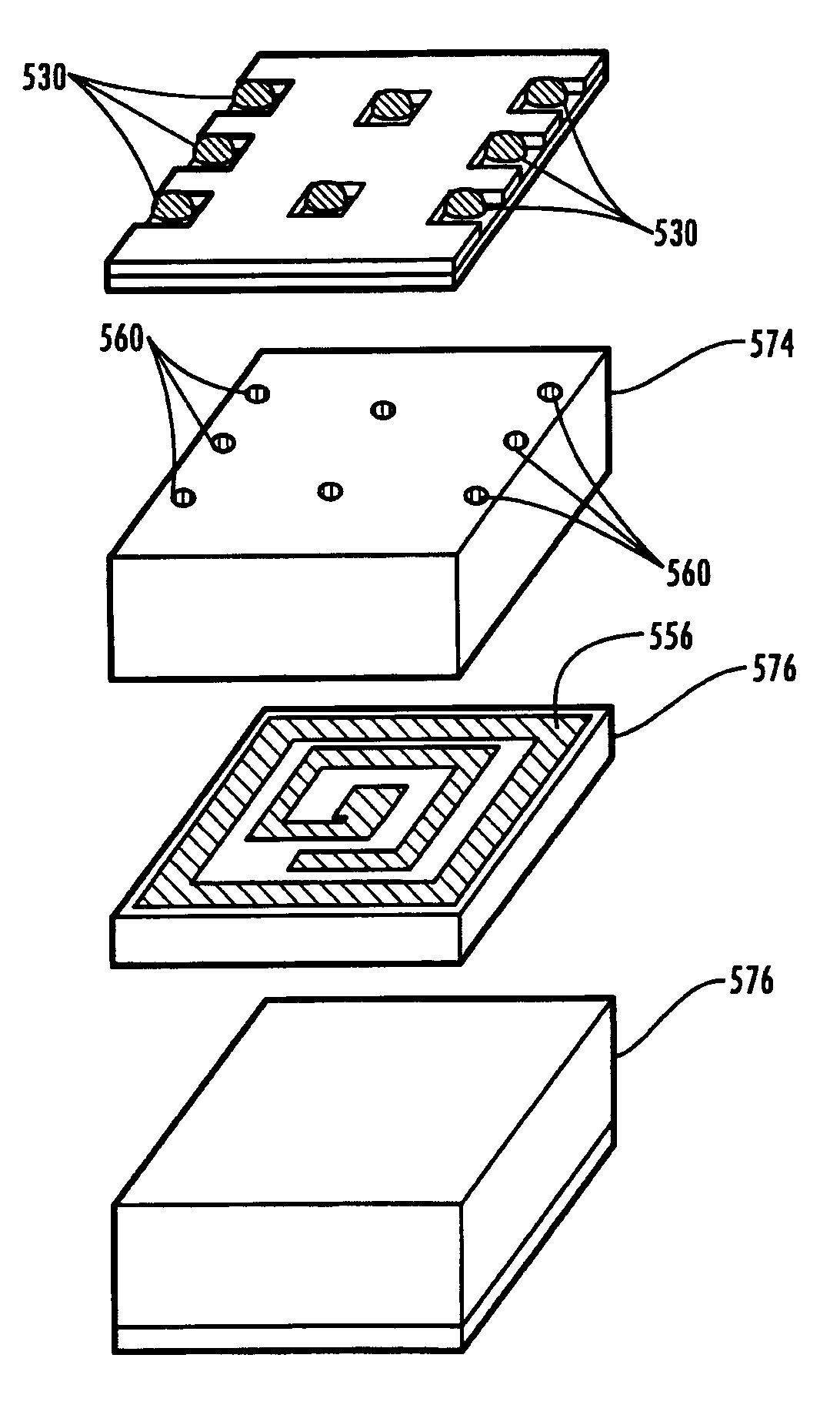
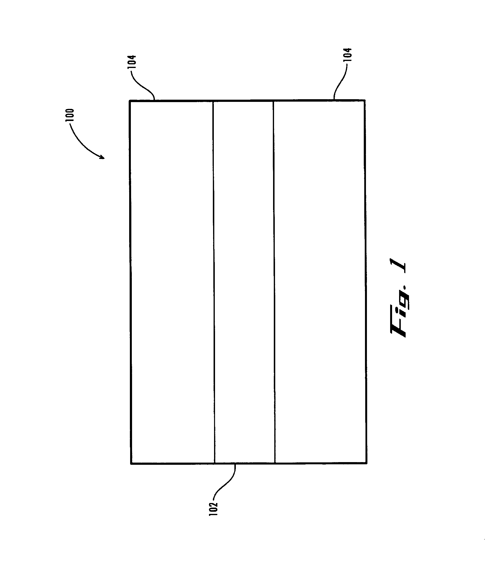
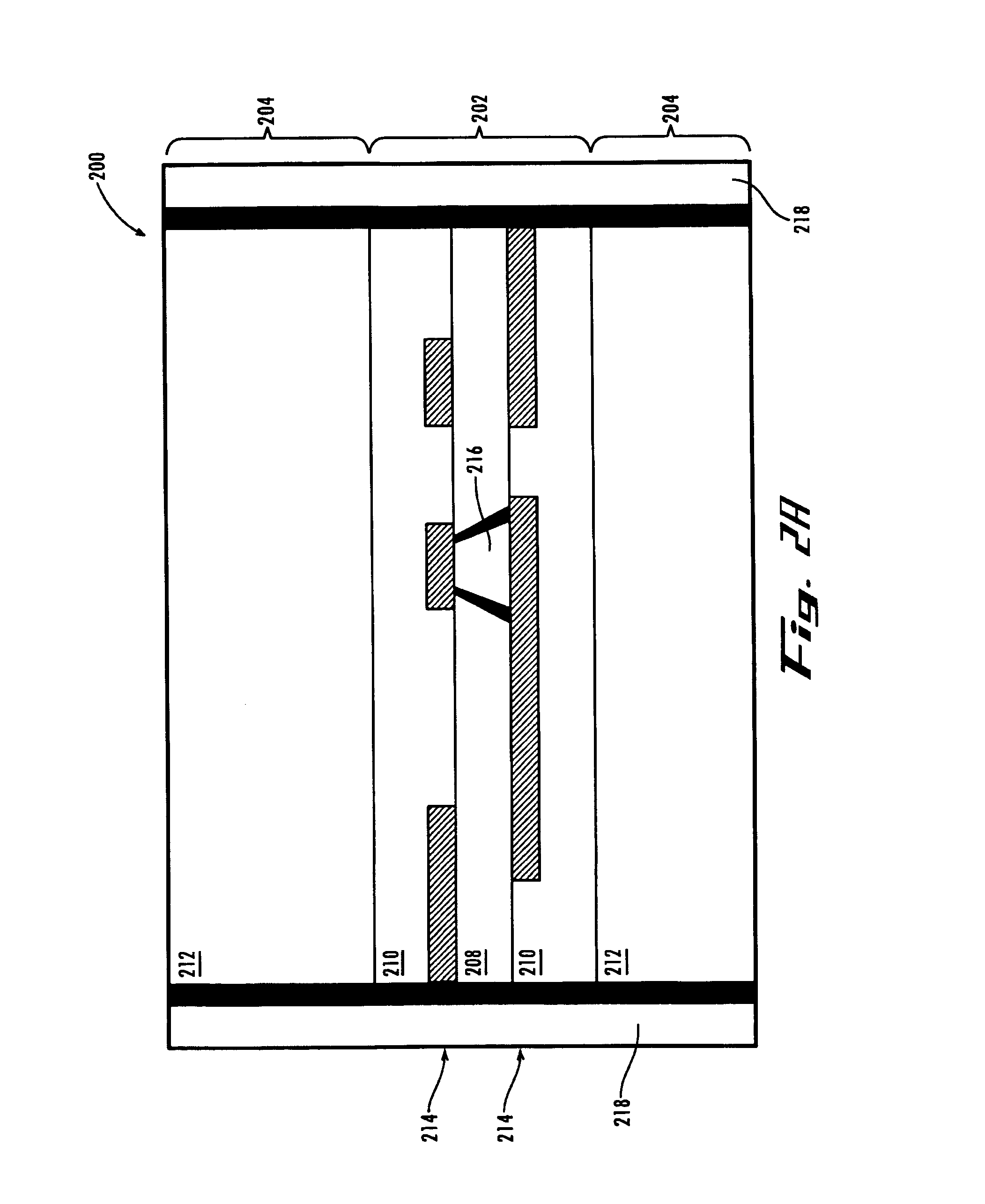
[0040]FIG. 1 is a schematic illustration of an embodiment of an all organic integrated passive device 100 packaged in a stand-alone configuration in accordance with an embodiment of the present invention. The device 100 comprises a device component 102 sandwiched between two shielding and packaging components 104. The device component 102 may comprise a single layer or multiple layers of low cost, high performance organic material metalized on one or both sides to form one or more passive devices, such as inductors, as discussed in more detail below. The shielding and packaging components 104 may comprise external shielding, particularly if the device component 102 does not provide in-built shielding, and / or one or more relatively thick and rigid structural layers, also referred to as core layers. The shielding and packaging layer 104 may comprise a single layer or multiple layers of material, as discussed in more detail below.

[0...


PUM


Abstract

The present invention provides for low cost discrete inductor devices in an all organic platform. The inductor devices can utilize virtually any organic material that provides the desired properties, such as liquid crystalline polymer (LCP) or polyphenyl ether (PPE), in a multilayer structure, wherein the organic materials have low moisture uptake and good temperature stability. Each layer may be metalized and selectively interconnected by vias formed in respective layers so as to form winding or coiled inductors. The inductor devices may advantageously include external shielding formed by metalizing the side walls and top surface of the inductor devices on in-built shielding achieved by the utilization of the hybrid co-planar waveguide topologies. The inductor devices can be configured for either ball grid array (BGA)/chip scale package (CSP) or surface mount device (SMD) mounting to circuit boards.

Description

STATEMENT OF GOVERNMENT INTEREST[0001]The work that led to this invention has been supported in part by a grant from the U.S. Army, Contract No. DAAH01-99-D-R002-0032. Thus, the United States Government may have certain rights to this invention.CROSS-REFERENCE TO RELATED APPLICATION[0002]This application is related to the following co-pending, commonly assigned U.S. applications, each of which is entirely incorporated herein by reference: “Methods for Fabricating Three-Dimensional All Organic Interconnect Structures” filed Mar. 28, 2003, and accorded application Ser. No. 10 / 402,315; and “Integrated Passive Devices Fabricated Utilizing Multi-Layer, Organic Laminates” filed Mar. 28, 2003, and accorded application Ser. No. 10 / 402,313.TECHNICAL FIELD[0003]The present invention is generally related to integrated passive devices formed as discrete components for use on circuit boards and, more particularly, is related to multilayer organic passive devices, such as inductors, for use in br...

Claims


Application Information

Patent Timeline
IPC IPC(8): H01L23/12H01L29/00H01L23/552H01L23/053H01F17/00H01F41/04H01L21/48H01L25/065H01L27/08H01P3/08H03H7/38
CPCH01F17/0006H01F41/041H01L21/4857H01L25/0652H01L27/08H01F17/0033H01L2924/0002H01L2924/09701H01L2924/3011H01L2924/00
Inventor WHITE, GEORGE E.SWAMINATHAN, MADHAVANSUNDARAM, VENKATESHDALMIA, SIDHARTH
Owner GEORGIA TECH RES CORP
Why Eureka
Try Eureka