
Register controlled delay locked loop with low power consumption

a register controlled and power consumption-reducing technology, applied in the field of semiconductor devices, can solve the problems of more power consumption, conventional register controlled dll has a drawback in signal integrity, etc., and achieve the effect of reducing the load of delayers and reducing power consumption

Inactive Publication Date: 2006-02-07
SK HYNIX INC
View PDF10 Cites 19 Cited by
  • Summary
  • Abstract
  • Description
  • Claims
  • Application Information

AI Technical Summary

Benefits of technology

[0016]It is, therefore, a primary object of the present invention to provide a digital locked loop (DLL) capable of minimizing power consumption in a DDR SDRAM (Double Data Rate Synchronous DRAM).
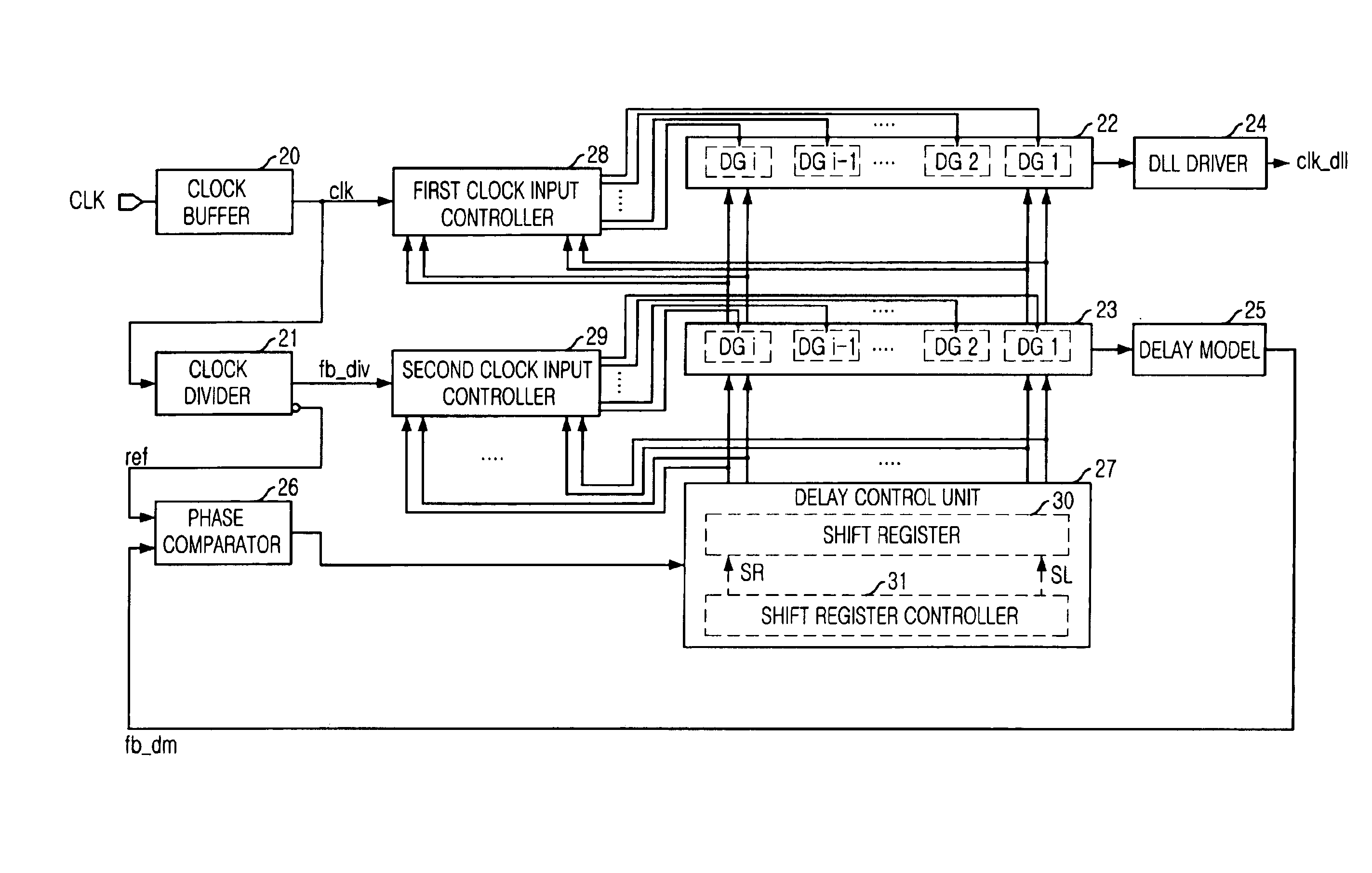
[0019]In the present invention, a delay line is divided into a plurality of delay groups, each of which has a plurality of unit delayer. One of the plurality of delay groups is driven by an output signal of a delay control unit. As a result, total amount of a load of the delayers is reduces in an operation mode. Since the delay line to which a source clock signal is applied is needed in an actual read operation, a control logic circuit is provided in the present invention in order that the source clock signal is transferred to the delay line in response to a read section signal, thereby reducing power consumption.

Problems solved by technology

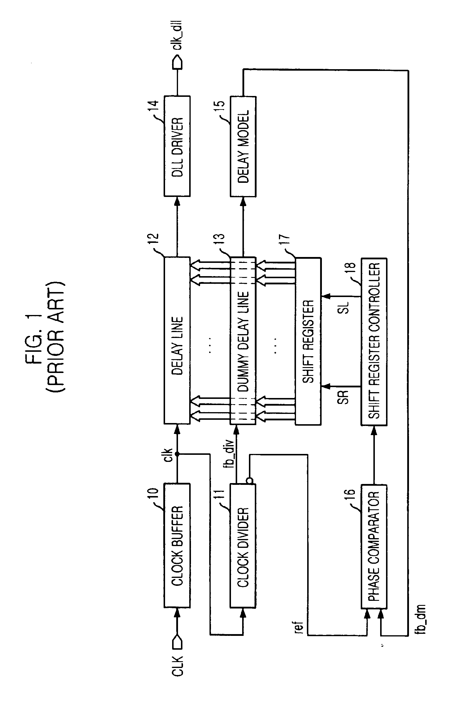
For example, since the conventional register DLL drives the delay line beside the read operation, the more power consumption is caused in the conventional register controlled DLL.
Further to the above-mentioned power consumption, the conventional register controlled DLL has a drawback in the signal integrity.
These problems appear in other digital DLL as well as the above-mentioned register controlled DLL.

Method used


Image

  • Register controlled delay locked loop with low power consumption
  • Register controlled delay locked loop with low power consumption
  • Register controlled delay locked loop with low power consumption

Examples


Embodiment Construction

[0031]Hereinafter, a digital DLL for a SDRAM according to the present invention will be described in detail accompanying the drawings.

[0032]First, referring to FIG. 5, the digital DLL according to the present invention includes a clock buffer 20, a clock divider 21, a phase comparator 26, a delay line 22, first and second clock input controllers 28 and 29, a dummy delay line 23, a delay control unit 27, a DLL driver 24, and a delay model 25.

[0033]The clock buffer 20 buffers an external clock signal CLK and generates a source clock signal clk which is synchronized with a rising or falling edge of the external clock signal CLK. The clock divider 21 divides the source clock signal clk into M (integer, typically M=8) divided clock signals and generates a monitoring clock signal fb_div and a reference clock signal ref. The delay line 22, which includes a plurality of delay groups having programmable unit delayers, delays the source clock signal clk from the clock buffer 20. The dummy del...


PUM


Abstract

The present invention relates to a digital delay locked loop (DLL) in DDR SDRAM (Double Data Rate Synchronous DRAM). The digital delay locked loop according to the present invention includes: first and second delay lines, each of which includes a plurality of delay groups, for delaying a source clock signal and a delay monitoring signal, wherein each of the delay groups include a plurality of programmable unit delayers; a delay model receiving an output signal of the second delay line for modeling a delay component of a clock signal path; a comparator for comparing a feedback clock signal from the delay model with a reference clock signal; a delay controller for controlling an amount of delay time of the first and second delay lines in response to a comparison result of the comparator; and first and second clock input controllers, which selectively provides the source clock signal and the delay monitoring clock signal to one of delay groups in the first and second delay lines, respectively, in response to output signals of the delay controller.

Description

FIELD OF THE INVENTION[0001]The present invention relates to a semiconductor device; and, more particularly, to a digital delay locked loop (DLL) in a Double Data Rate Synchronous (DRAM DDR SDRAM).BACKGROUND OF THE INVENTION[0002]Generally, a clock signal has been used as a reference signal which is synchronized with an operation timing in a system or an electronic circuit and this clock signal has been used for high-speed performance of an integrated circuit without an error. When a clock signal from an external circuit is used in an internal circuit, a delay of the clock signal, which is said “clock skew”, is generated in the internal circuit. To prevent this skew in the internal circuit, a DLL to synchronize an internal clock signal with an external clock signal has been employed.[0003]On the other hand, as compared with a conventional phase locked loop (PLL), the DLL has a merit in that it has an effect on the noise so that the DLL has been used in SDRAMs (Synchronous DRAM) and ...

Claims


Application Information

Patent Timeline
IPC IPC(8): H03L7/06G06F1/12G06F1/10G11C11/407G11C11/4076H03K5/00H03K5/131H03K5/14H03L7/081
CPCH03K5/131H03K5/133H03L7/0814H03K2005/00058G11C11/407
Inventor LEE, JAE-JIN
Owner SK HYNIX INC
Learn More