Optimized buffering for JTAG boundary scan nets

a technology of buffering, which is applied in the direction of individual semiconductor device testing, semiconductor/solid-state device testing/measurement, instruments, etc., can solve the problems of increasing congestion, chain failure, and current netlists which go into layout do not contain sufficient buffering of high fanout jtag boundary scan control nets

Inactive Publication Date: 2006-02-14
AVAGO TECH WIRELESS IP SINGAPORE PTE
View PDF14 Cites 17 Cited by
  • Summary
  • Abstract
  • Description
  • Claims
  • Application Information

AI Technical Summary

Benefits of technology

[0007]The objects, features and advantages of the present invention include providing a method and / or architecture for implementing optimized buffering for JTAG boundary scan nets that may (i) buffer scan nets in a way which reflects the order of the I / Os around the die, (ii) allow buffering cell placement and net routing tools to achieve optimal results automatically, (iii) provide universal JTAG boundary scan designs, (vi) implement boundary scan cells inside the I / O cells, (v) implement boundary scan flip flops without a clock tree, (vi) meet hold times for the boundary scan chain, (vii) reduce crosstalk and noise impact of the scan connection, (viii) improve flip flop performance, (ix) provide power savings, (x) reduce turnaround time, and / or (xi) have no additional area cost.

Problems solved by technology

Because there are several control nets which can go to each I / O cell (not shown, surrounding the ASIC 10), uncontrolled routing occurs and increases congestion problems.
However, current netlists which go into layout do not contain sufficient buffering of the high fanout JTAG boundary scan control nets.
Furthermore, each design has to be handled individually, since no common solution exists.
Trying to connect the boundary scan cells 22a–22n, which are scattered over the entire die, can cause timing problems.
Since the boundary scan flip flops are connected in a chain, routing issues cause severe hold time violations, thereby causing the chain to fail.
However, placing the boundary scan cells 22a–22n manually is very time consuming (there typically exist hundreds of cells in a single device).
For example, the manual placement process can take a number of days in a standard size design.
Therefore, managing a reasonable skew at chip level is challenging, time consuming and area consuming.

Method used


Image

  • Optimized buffering for JTAG boundary scan nets
  • Optimized buffering for JTAG boundary scan nets
  • Optimized buffering for JTAG boundary scan nets

Examples


Embodiment Construction

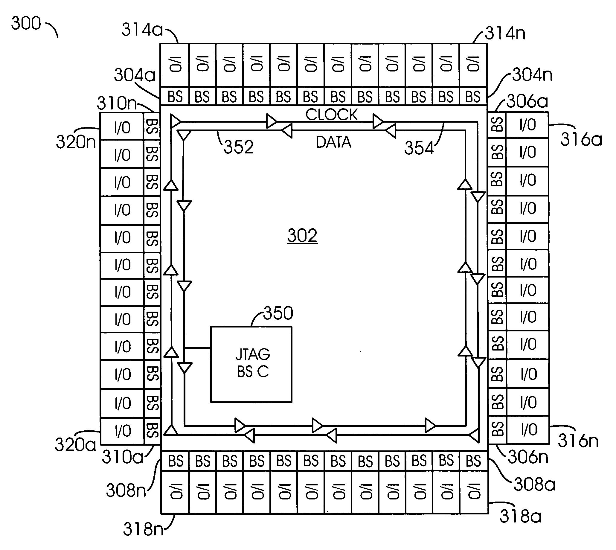
[0018]Referring to FIG. 3, a block diagram of a system (or circuit) 100 is shown in accordance with a preferred embodiment of the present invention. The circuit 100 may be configured to improve the overall routing of JTAG boundary scan control nets in an ASIC design. The circuit 100 may be configured to reduce the area which is needed for the net routing and to provide control of where wires will be located on the die after final layout is completed. The system 100 may be configured to optimize buffering for JTAG boundary scan nets. An example of a JTAG boundary scan net may be found in the IEEE Standard Test Access Port and Boundary-Scan Architecture, published Feb. 15, 1990 and revised on Jun. 17, 1993, which is hereby incorporated by reference in its entirety.

[0019]The system 100 generally comprises a JTAG boundary scan controller 102, a number of buffers 104a–104n, a number of buffers 106a–106n, a number of cells 108a–108n, a number of cells 110a–110n, a number of cells 112a–112...


PUM


Abstract

An apparatus comprising one or more groups of boundary scan cells, one or more group buffers, one or more repeater buffers and a controller. The group buffers may be coupled to each of the groups of boundary scan cells. The repeater buffers may be coupled in series with the group buffers. The controller may be coupled to the groups of boundary scan cells through the group buffers and the repeater buffers. The apparatus may be configured to buffer the groups of boundary scan cells to reflect an order of I / Os around the apparatus.

Description

FIELD OF THE INVENTION[0001]The present invention relates to a method and / or architecture for improving implementing JTAG boundary scan control nets generally and, more particularly, to a method and / or architecture for (i) reducing the area which is needed for the net routing and (ii) controlling placement of wires on the die after final layout is completed.BACKGROUND OF THE INVENTION[0002]Referring to FIG. 1, a conventional JTAG boundary scan control signal routing of an application specific integrated circuit (ASIC) 10 is shown. The JTAG signal routing of the ASIC 10 is buffered in a tree structure. The starting point for the tree is typically located somewhere in the center region of the die. In some instances the JTAG boundary scan gates can be placed elsewhere manually. From the starting point the trees fan out to all different sides of the ASIC 10. Therefore, the ASIC 10 will have JTAG boundary scan signal buffers all over the die. Also, routes will go through the center of th...

Claims


Application Information

Patent Timeline
Patent Type & Authority Patents(United States)
IPC IPC(8): G01R31/28
CPCG01R31/318572G01R31/318541
Inventor DIRKS, JUERGENLAHNER, JUERGEN K.JOHANTERWAGE, LUDGER F.MBOUOMBOUO, BENJAMINBOLUKI, HUMANLI, WEIDAN
Owner AVAGO TECH WIRELESS IP SINGAPORE PTE
Why Eureka
Try Eureka