
Hydrogen-based phosphosilicate glass process for gap fill of high aspect ratio structures

a phosphosilicate glass and hydrophobic technology, applied in the direction of basic electric elements, semiconductor/solid-state device manufacturing, electric apparatus, etc., can solve the problems of reducing budgets, void-free filling of high aspect ratio spaces (e.g., ar>3:1) becomes increasingly difficult, and the top part of a high aspect ratio structure sometimes closes, etc., to achieve reduced side-wall dielectric redeposition, enhanced mobility of the dielectric, and reduced red

Inactive Publication Date: 2006-02-21
NOVELLUS SYSTEMS
View PDF20 Cites 33 Cited by
  • Summary
  • Abstract
  • Description
  • Claims
  • Application Information

AI Technical Summary

Benefits of technology

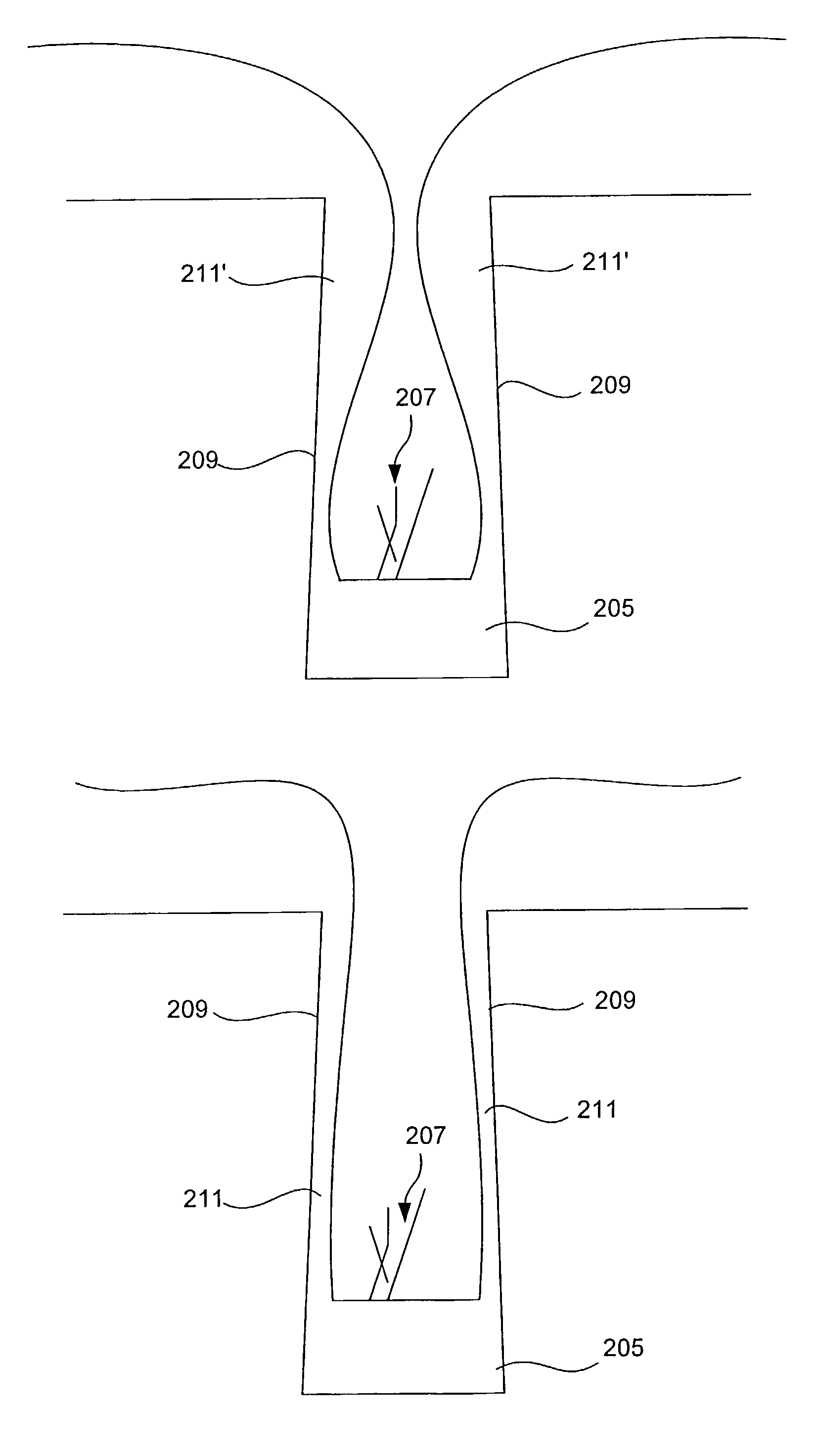
[0009]This invention addresses that need by providing hydrogen as a PSG process gas in a high density plasma CVD process. This process has been found to provide void free high-quality gap filling with phosphorus-containing dielectric materials. These benefits occur even in very narrow, high aspect ratio features.
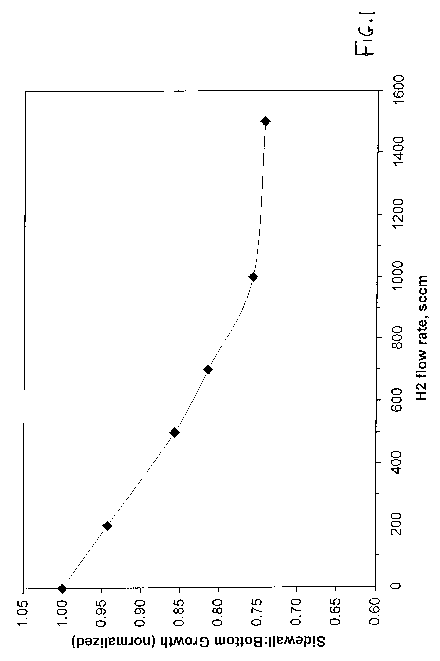
[0011]The process gas preferably provides hydrogen (H2) at a flow rate of at least about 400 sccm and phosphine (PH3) at a flow rate of at least about 0.5 sccm. In a specific embodiment, a process gas having a hydrogen flow rate of about 1000 sccm and a phosphine flow rate of about 8 sccm is used. These values are based on a 200 millimeter substrate. Larger substrates may require correspondingly higher flow rates. The inventors have found that hydrogen flow rates in this regime provide significantly reduced side-wall dielectric redeposition and that phosphine flow rates in this range provide in situ etch of the overhang at the entry region of the trench and enhanced mobility of the dielectric during HDP CVD.
[0012]In a preferred embodiment, the substrate is heated to a temperature of between about 300 and 680° C., for example between about 450 and 550° C., and held in this temperature range during the deposition process. While improved results from hydrogen addition are present over a much wider range of temperatures, this temperature range in particular has been found to provide superior results.

Problems solved by technology

As device geometries shrink and thermal budgets are reduced, void-free filling of high aspect ratio spaces (e.g., AR>3:1) becomes increasingly difficult due to limitations of existing deposition processes.
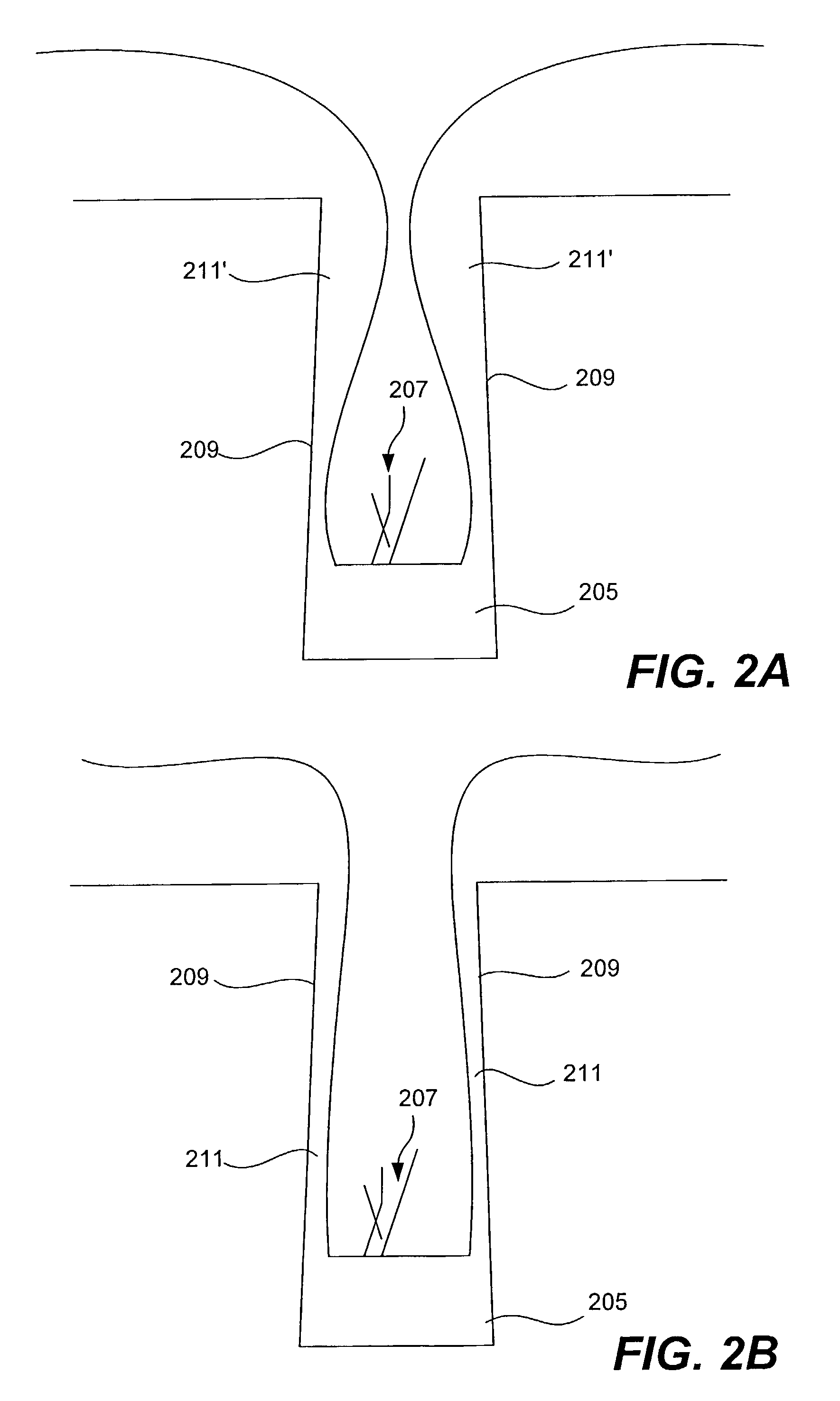
As a result the top part of a high aspect ratio structure sometimes closes prematurely leaving voids within the gap's lower portions.
This problem is exacerbated in small features.
Furthermore, as aspect ratios increase, the shape of the gap itself can contribute to the problem.
High aspect ratio gaps often exhibit reentrant features, which make gap filling even more difficult.
The most problematic reentrant feature is a narrowing at the top of the gap.
Hence voids and seams become even more likely.
However, boron is an otherwise undesirable component of the fill material, prone to forming hygroscopic layers.
Furthermore, BPSG processes (and the like) are expiring due to incompatibility with the advanced device constraint of a maximum thermal budget of about 700° C.
Thus, HDP CVD is not an entirely diffusion-based (isotropic) process.
Nevertheless, some overhang still results at the entry region of the gap to be filled.
Thus, the formation of overhang cannot be totally eliminated and is inherent to the physics and chemistry of the HDP CVD process.
Of course, limitations due to overhang formation become ever more severe as the width of the gap to be filled decreases, the aspect ratio increases, and the features become reentrant.

Method used


Image

  • Hydrogen-based phosphosilicate glass process for gap fill of high aspect ratio structures
  • Hydrogen-based phosphosilicate glass process for gap fill of high aspect ratio structures
  • Hydrogen-based phosphosilicate glass process for gap fill of high aspect ratio structures

Examples


example 1

[0077]FIG. 5 shows FTIR absorbance spectra for dielectric films deposited by a standard PSG HDP CVD process (502) and a hydrogen containing PSG process using 200, 500 and 1000 sccm H2 (504, 506 and 508, respectively). Importantly, all of the curves have peaks with almost identical spectral locations and magnitudes. This result indicates that the dielectric formed by a hydrogen-based PSG process in accordance with the present invention has acceptable optical properties relative to the standard PSG dielectric. Also, note that there are no peaks associated with Si—H, H2O, or SiO—H. Each of these detrimental species could potentially form when hydrogen is present. The films were deposited using the following conditions:

[0078]

Standard PSG ProcessSiH492 sccmO2235 sccmPH348 sccmH20 sccmHe100 sccmLF Power3750 WattsHF Power2250 Watts

[0079]

H-Based PSG ProcessSiH430 sccmO265 sccmPH38 sccmH2200, 500, 1000 sccm, respectivelyHe0 sccmLF Power4000 WattsHF Power1300 Watts

example 2

[0080]FIG. 6 shows a bar graph representing the maximum aspect ratio capable of void free fill with and without hydrogen in a PSG process gas. The HPD CVD conditions used were the same as those noted above in connection with FIG. 5 (for the H-based process, 1000 sccm H was used). The bar on the left represents the achievable aspect ratio fill for the standard PSG process without hydrogen. The bar on the right represents the achievable aspect ratio fill for the H-based PSG process. The results show that a substantial increase in the aspect ratio that may be filled with a PSG process gas is achieved by using an H-based PSG process in accordance with the present invention.


PUM


Abstract

Chemical vapor deposition processes are employed to fill high aspect ratio (typically at least 3:1), narrow width (typically 1.5 microns or less and even sub 0.13 micron) gaps with significantly reduced incidence of voids or weak spots. This deposition process involves the use of hydrogen and a phosphorus dopant precursor as process gasses in the reactive mixture of a plasma containing CVD reactor. The process gas also includes dielectric forming precursor molecules such as silicon and oxygen containing molecules.

Description

CROSS-REFERENCE TO RELATED APPLICATION[0001]This application claims priority from prior U.S. Patent Application Ser. No. 09 / 996,619, now U.S. Pat. No. 6,596,654 titled “GAP FILL FOR HIGH ASPECT RATIO STRUCTURES,” filed Nov. 28, 2001 by Bayman et al; which claims priority to U.S. Provisional Patent Application 60 / 310,004, titled “GAP FILL FOR HIGH ASPECT RATIO STRUCTURES,” filed Aug. 3, 2001 by Bayman et al. Both of these prior patent applications are incorporated herein by reference for all purposes.BACKGROUND OF THE INVENTION[0002]This invention relates to electronic device fabrication processes and associated apparatus. More specifically, the invention relates to chemical vapor deposition processes for forming dielectric layers in high aspect ratio, narrow width recessed features.[0003]It is often necessary in semiconductor processing to fill a high aspect ratio gaps with insulating material. This is the case for shallow trench isolation, inter-metal dielectric layers, passivation...

Claims


Application Information

Patent Timeline
Patent Type & Authority Patents(United States)
IPC IPC(8): H01L21/31H01L21/311H01L21/469H01L21/314H01L21/316H01L21/762
CPCH01L21/02126H01L21/02129H01L21/02131H01L21/0214H01L21/02164H01L21/02274H01L21/76224H01L21/0234H01L21/3144H01L21/3145H01L21/31608H01L21/31625H01L21/31629H01L21/0228H01L21/02211
Inventor PAPASOULIOTIS, GEORGE D.RAHMAN, MD SAZZADURSUN, PIN SHENGPRICHARD, KARENHALL, LAURENSINGH, VIKRAM
Owner NOVELLUS SYSTEMS
Learn More