Semiconductor light emitting device integral type semiconductor light emitting unit image display unit and illuminating unit

semiconductor technology, applied in the direction of semiconductor devices, basic electric elements, electrical appliances, etc., can solve the problems of silicon-based material, obstructing the improvement of luminous efficiency of the light emitting diode, and the above-described light emitting diode, so as to facilitate the fabrication of a semiconductor light emitting device and improve luminous efficiency , the effect of improving luminous efficiency

Active Publication Date: 2006-02-21
SAMSUNG ELECTRONICS CO LTD
View PDF5 Cites 420 Cited by
  • Summary
  • Abstract
  • Description
  • Claims
  • Application Information

AI Technical Summary

Benefits of technology

[0006]An advantage of the present invention is to provide a method of fabricating a semiconductor light emitting device, which is capable of easily fabricating a semiconductor light emitting device with the significantly improved luminous efficiency.
[0007]Another advantage of the present invention is to provide a semiconductor light emitting device with the significantly improved luminous efficiency.
[0008]A further advantage of the present invention is to provide a method of fabricating an image display unit, which is capable of fabricating an image display unit with the significantly improved luminous efficiency, and to provide an image display unit with the significantly improved luminous efficiency.
[0009]Yet a further advantage of the present invention is to provide a method of fabricating an illuminating unit, which is capable of fabricating an illuminating unit with the significantly improved luminous efficiency, and to provide an illuminating unit with the significantly improved luminous efficiency.
[0010]According to an embodiment of the present invention, there is provided a method of fabricating a semiconductor light emitting device, including the steps of growing a first semiconductor layer of a first conductive type on a substrate; forming a growth mask having an opening at a ...

Problems solved by technology

The above-described light emitting diode, however, has a problem.
Although silicon oxide (SiO2) or silicon nitride (SiN) is generally used as the material of the growth mask for selective growth, the use of such a silicon-based material is disadvantageous in that since the selective growth of the n-type GaN layer and the subsequent growth of the p-type GaN layer are both performed at a temperature being as high as about 100° C., silicon (Si) and oxygen (O) are relea...

Method used


Image

  • Semiconductor light emitting device integral type semiconductor light emitting unit image display unit and illuminating unit
  • Semiconductor light emitting device integral type semiconductor light emitting unit image display unit and illuminating unit
  • Semiconductor light emitting device integral type semiconductor light emitting unit image display unit and illuminating unit

Examples


first embodiment

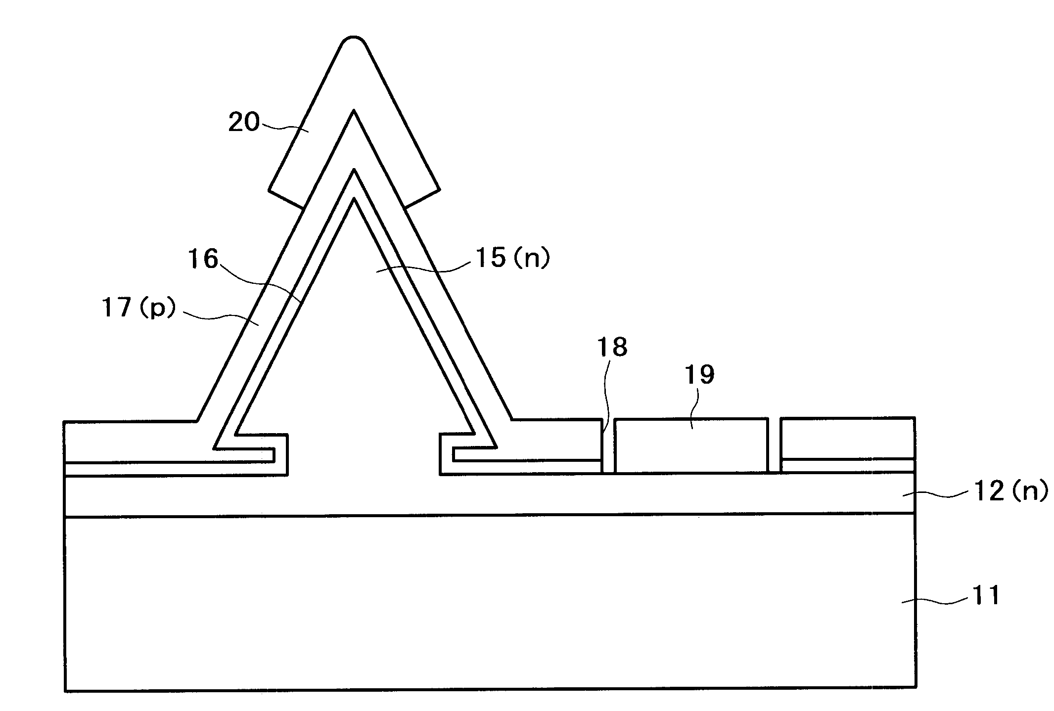
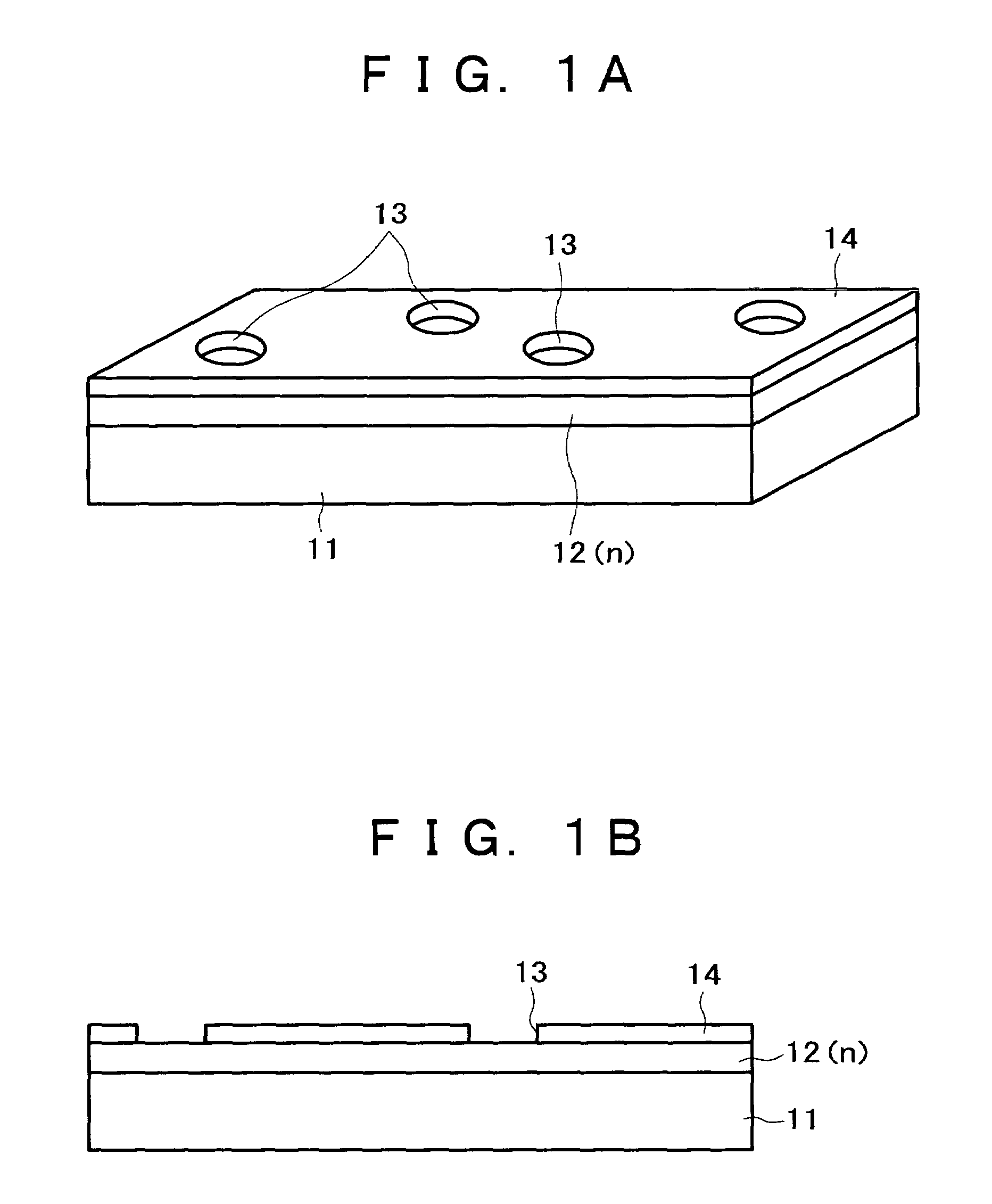
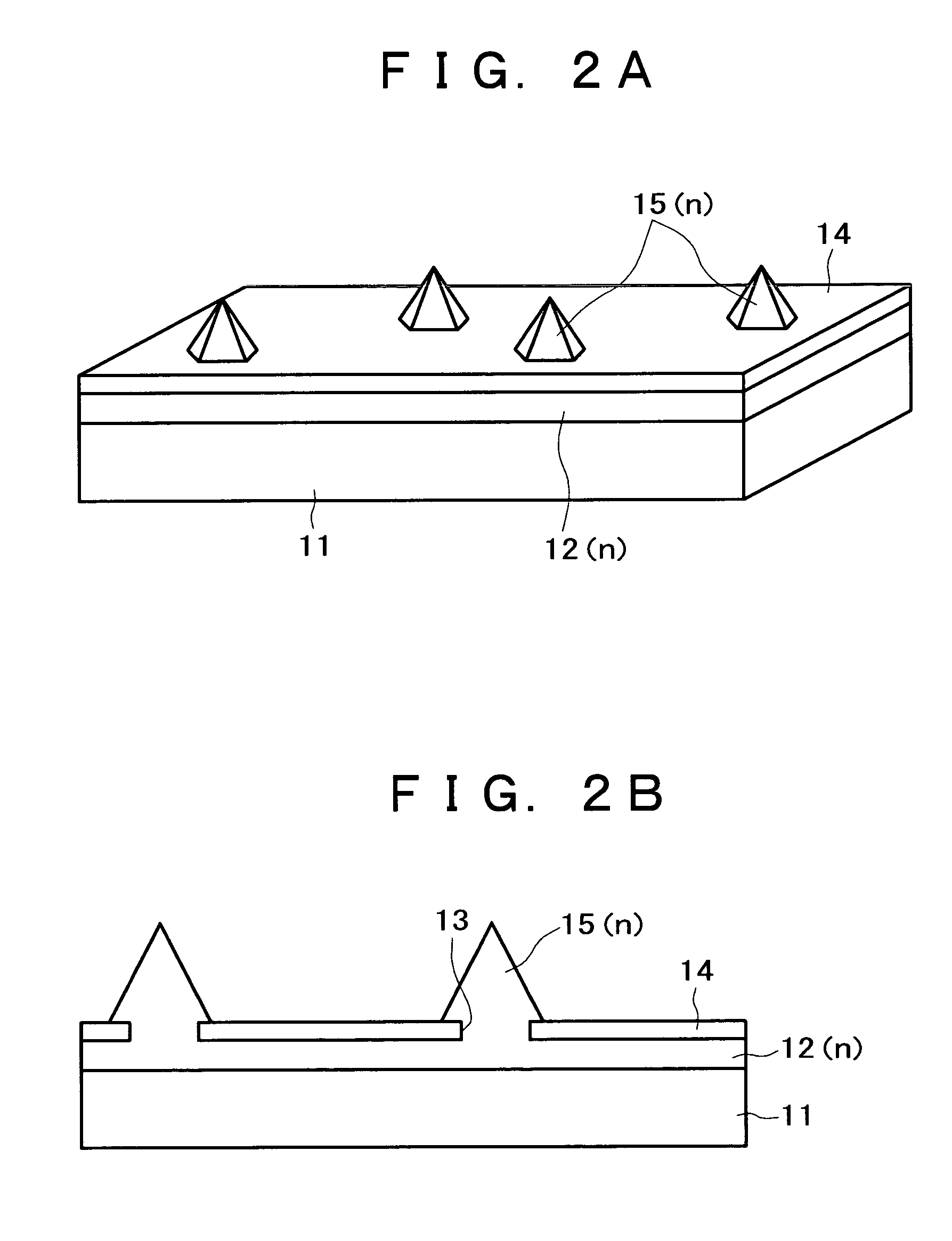
[0066]FIGS. 1A to 6B show sequential steps of a process of fabricating a GaN based light emitting diode according to the present invention, wherein FIGS. 1A, 2A, 3A, 4A, 5A and 6A are perspective views and FIGS. 1B, 2B, 3B, 4B, 5B, and 6B are sectional views; and FIG. 7 is a sectional view showing a final state of the GaN based light emitting diode fabricated by the fabrication process shown in FIGS. 1A to 6B.

[0067]FIGS. 1A and 1B show a step of forming a growth mask. A sapphire substrate 11 with the C+-plane of sapphire taken as the principal plane is prepared. The surface of the sapphire substrate 11 is cleaned, for example, by thermal cleaning. An n-type GaN layer 12 doped with Si representative of an n-type impurity is grown on the cleaned surface of the sapphire substrate 11, for example, by a MOCVD (Metal Organic Chemical Vapor-phase Deposition) process. The n-type GaN layer 12 is preferably grown in such a manner that the density of crystal defects, particularly, threading di...

second embodiment

[0094]A GaN based light emitting diode according to the present invention will be described below with reference to FIG. 13.

[0095]In the second embodiment, as shown in FIG. 13, a p-side electrode 20 is not formed in the vicinity of the top of a hexagonal pyramid shaped p-type GaN layer 17 but is formed to cover only middle portions of tilt planes of the layer 17. To be more specific, the size of the p-side electrode 20 is set in a range of about 50% or less of the size of the hexagonal pyramid shaped p-type GaN layer 17 and the p-side electrode 20 is not formed in the vicinity of the top of the layer 17. As a result of observation using an AFM (Atomic Force Microscope), it is apparent that the crystallinity of a portion, in the vicinity of the top, of the hexagonal pyramid shaped p-type GaN layer 17 is poorer than that of another portion. From this viewpoint, according to this embodiment, the p-side electrode 20 is formed in a region, excluding the top and its neighborhood in which ...

third embodiment

[0097]A GaN based light emitting diode according to the present invention will be described below with reference to FIGS. 14 and 15.

[0098]The same steps as those in the first embodiment are repeated until a p-type GaN layer 17 is grown on a hexagonal pyramid shaped structure, and then a p-side electrode 20 is formed on the p-type GaN layer 17. The stacked layer structure, which includes the n-type GaN layer 12 and the hexagonal pyramid shaped structure formed thereon, is peeled from the sapphire substrate 11 by irradiating the sapphire substrate 11 with laser beams such as excimer laser beams from the back surface side of the sapphire substrate 11. The back surface of the n-type GaN layer 12 of the stacked layer structure thus peeled is flattened by etching or the like, and as shown in FIG. 14, an n-side electrode 19 is formed on the back surface of the n-type GaN layer 12. The n-side electrode 19 may be configured as a transparent electrode made from ITO (Indium Tin Oxide). In this...


PUM


Abstract

A semiconductor light emitting device with improved luminous efficiency is provided. An underlying n-type GaN layer is grown on a sapphire substrate, and a growth mask made from SiO2 film or the like is formed on the underlying n-type GaN layer. An n-type GaN layer having a hexagonal pyramid shape is selectively grown on a portion, exposed from an opening of the growth mask, of the underlying n-type GaN layer. The growth mask is removed by etching, and then an active layer and a p-type GaN layer are sequentially grown on the entire substrate so as to cover the hexagonal pyramid shaped n-type GaN layer, to form a light emitting device. An n-side electrode and a p-side electrode are then formed.

Description

CROSS REFERENCE RELATED TO APPLICATIONS[0001]This patent application claims priority to Japanese Patent Document No. P2002-261407 filed on Sep. 6, 2002, the disclosure of which is herein incorporated by reference.BACKGROUND OF THE INVENTION[0002]The present invention relates to a semiconductor light emitting device and a fabrication method thereof, an integral type semiconductor light emitting unit and a fabrication method thereof, an image display unit and a fabrication method thereof, and an illuminating unit and a fabrication method thereof. In particular, the present invention is suitably applied to light emitting diodes using nitride oxide type III–V compound semiconductors.[0003]A related art light emitting diode representative of a semiconductor light emitting device as disclosed in WO02 / 07231 (see, for example pages 47–50, FIGS. 3 to 9), is configured by growing an underlying n-type GaN layer on a sapphire substrate, forming a growth mask having an opening at a specific posi...

Claims


Application Information

Patent Timeline
IPC IPC(8): H01L33/00H01L27/15H01L33/24
CPCH01L33/24H01L27/156H01L33/007H01L2224/48137
Inventor OKUYAMA, HIROYUKIBIWA, GOSHISUZUKI, JUN
Owner SAMSUNG ELECTRONICS CO LTD
Why Eureka
Try Eureka