Charged particle beam exposure apparatus and method

a charge particle and beam technology, applied in the field of charge particle beam exposure apparatus and charge particle beam exposure method, can solve the problems of reducing the precision of connecting patterns drawn by the respective charge particle beams, affecting the quality of charged particle beams, so as to achieve higher-precision drawing

Inactive Publication Date: 2006-02-28
CANON KK
View PDF15 Cites 33 Cited by
  • Summary
  • Abstract
  • Description
  • Claims
  • Application Information

AI Technical Summary

Benefits of technology

[0005]It is an object of the present invention to provide a charged particle beam exposure apparatus which corrects a change in positional relationship, occurring in accordance with, e.g., the density of a pattern to be drawn on a substrate, among charged particle beams, so that higher-precision drawing than in the conventional case can be realized.

Problems solved by technology

In this manner, when the positional relationship among the charged particle beams changes, the connecting precision among patterns drawn by the respective charged particle beams degrades, and a desired pattern cannot be formed at high precision.
Thus, when a pattern including a pattern with a high density and a pattern with a low density is to be drawn, the connecting precision among the patterns degrades.

Method used


Image

  • Charged particle beam exposure apparatus and method
  • Charged particle beam exposure apparatus and method
  • Charged particle beam exposure apparatus and method

Examples


first embodiment

[First Embodiment]

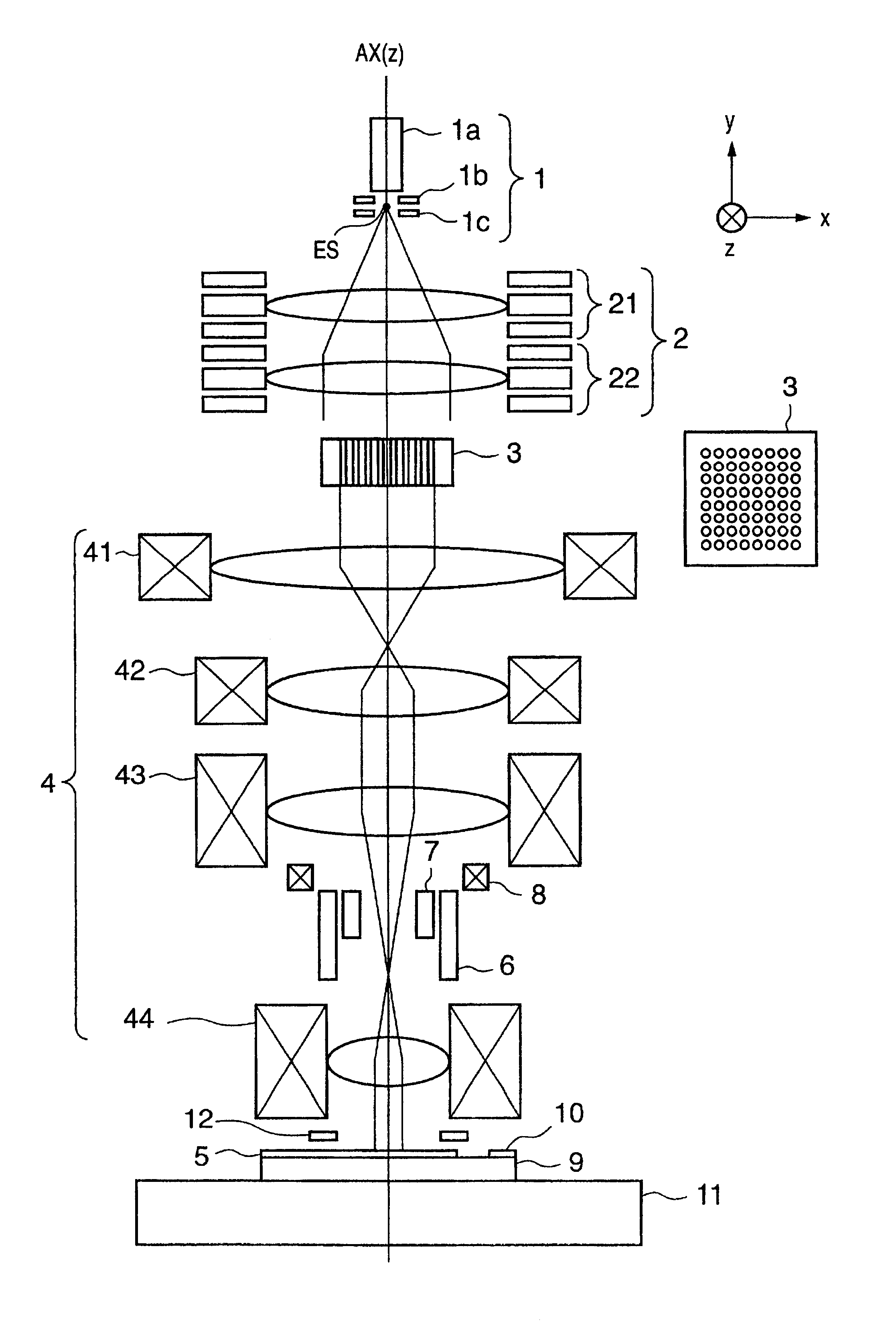
[0043]FIG. 1 is a view schematically showing the main part of an electron beam exposure apparatus according to the first embodiment of the present invention.

[0044]Referring to FIG. 1, reference numeral 1 denotes an electron gun constituted by a cathode 1a, grid 1b, and anode 1c. Electrons emitted from the cathode 1a form a cross-over image between the grid 1b and anode 1c. In the following description, this cross-over image is called an electron source ES.

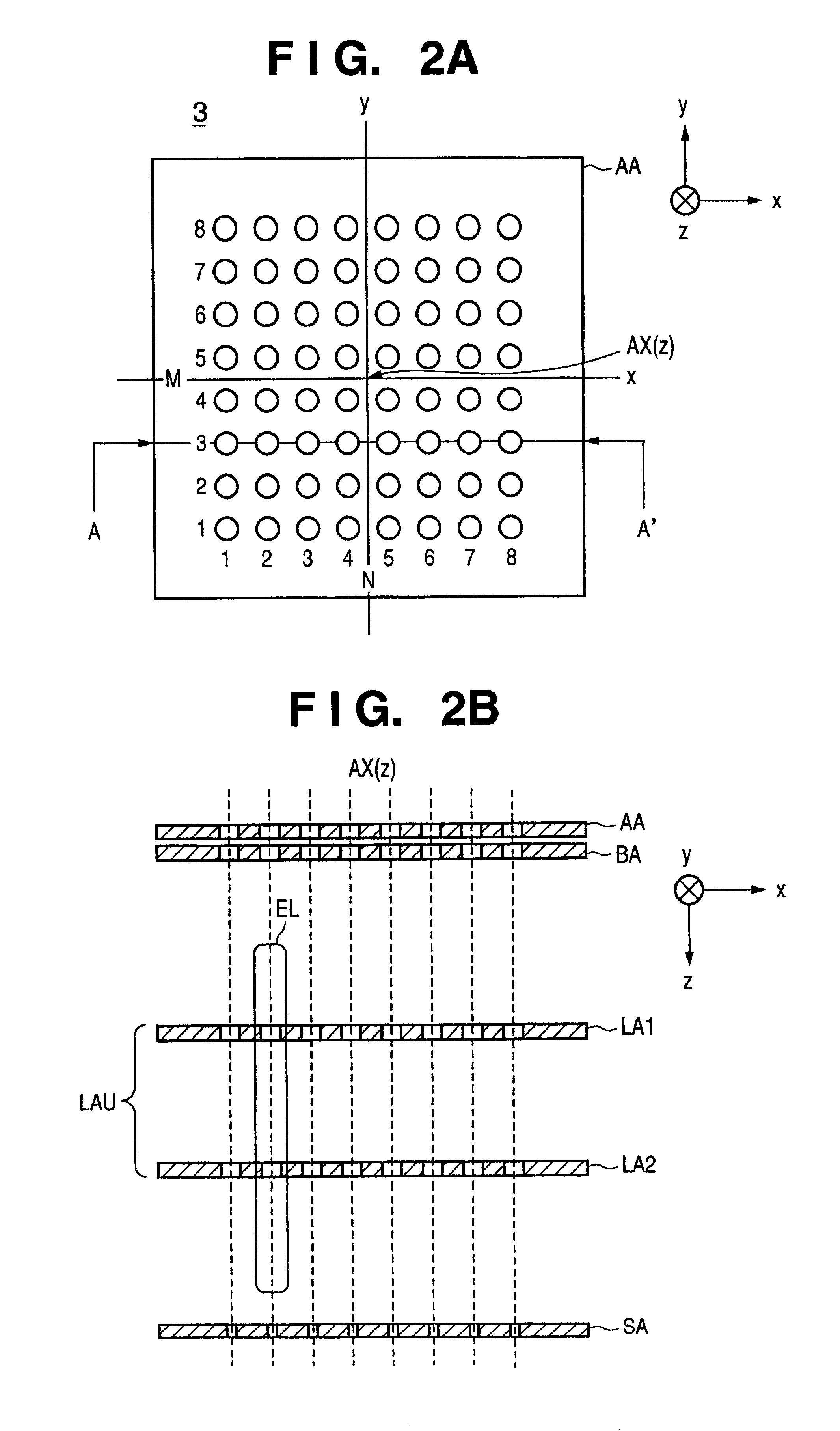
[0045]An electron beam emitted from the electron source ES irradiates an element electron optical system array 3 through a condenser lens 2. The condenser lens 2 according to this embodiment is comprised of electron lenses (unipotential lenses) 21 and 22 each made up of three aperture electrodes.

[0046]The element electron optical system array 3 forms a plurality of intermediate images of the electron source ES. The respective intermediate images are reduced and projected by a reduction electron optical system 4 (t...

second embodiment

[Second Embodiment]

[0089]FIG. 11 is a schematic view showing the main part of an electron beam exposure apparatus according to the second embodiment of the present invention. The same constituent elements as in the electron beam exposure apparatus of the first embodiment described above shown in FIG. 1 are denoted by the same reference numerals, and a detailed description thereof will be omitted.

[0090]In the second embodiment, a condenser lens 2 is formed of an electron lens comprising three aperture electrodes. Although the condenser lens 2 does not include unipotential lenses 21 and 22, which constitute one characteristic feature of the first embodiment, it may include them in the second embodiment as well.

[0091]An element electron optical system array 3 used in the electron beam exposure apparatus according to the second embodiment will be described with reference to FIGS. 12A and 12B. The same constituent elements as in the element electron optical system array 3 of the first em...

third embodiment

[Third Embodiment]

[0114]As the third embodiment of the present invention, a device manufacturing method using the electron beam exposure apparatus according to the first or second embodiment of the present invention will be described.

[0115]FIG. 20 shows the flow of manufacture of a microdevice (e.g., a semiconductor chip such as an IC or LSI, a liquid crystal panel, a CCD, a thin film magnetic head, a micromachine, or the like). In step 1 (design circuit), a semiconductor device circuit is designed. In step 2 (form exposure control data), the exposure control data of the exposure apparatus is formed on the basis of the designed circuit pattern. In step 3 (manufacture wafer), a wafer is manufactured by using a material such as silicon. In step 4 (wafer process), called a pre-process, an actual circuit is formed on the wafer by lithography using the exposure apparatus, to which the prepared exposure control data has been input, and the wafer. In step 5 (assembly), called a post-proces...


PUM

PropertyMeasurementUnit
densityaaaaaaaaaa
electron optical poweraaaaaaaaaa
photosensitiveaaaaaaaaaa

Abstract

A multi-charged-particle beam drawing apparatus and method that can correct a change in positional relationship, caused by the Coulomb effect, among charged particle beams are provided. The focal lengths of two electron lenses (21, 22) that form a condenser lens (2) are adjusted individually to change a relative positional relationship between the front focal position of the condenser lens (2) and an electron source (ES). Electron beams becoming incident on an aperture array (AA) can diverge, or be focused or collimated. Therefore, positions where intermediate images (img1-img3) are to be formed can be changed, and the change in positional relationship, caused by the Coulomb effect, among the charged particle beams can be corrected.

Description

FIELD OF THE INVENTION[0001]The present invention relates to a charged particle beam exposure apparatus and charged particle beam exposure method and, more particularly, to a charged particle beam exposure apparatus and charged particle beam exposure method of drawing a pattern on a substrate such as a wafer directly or drawing a pattern on a master such as a mask or reticle.BACKGROUND OF THE INVENTION[0002]In a charged particle beam exposure apparatus which performs exposure by causing a charged particle beam to form an image on a substrate, when the current of the charged particle beam is large, the image of the charged particle beam projected on the substrate is blurred by the Coulomb effect. Although most of the blur caused by the Coulomb effect can be corrected by readjusting the focal position of a reduction electron optical system for charged particle beam projection, an uncorrected blur component remains. Conventionally, the blur to be caused by the Coulomb effect is predict...

Claims


Application Information

Patent Timeline
Patent Type & Authority Patents(United States)
IPC IPC(8): G21K5/10H01J37/08G03F7/20H01J37/147H01J37/153H01J37/302H01J37/305H01J37/317H01L21/027
CPCB82Y10/00B82Y40/00H01J37/3177H01J37/302H01J2237/30461
Inventor MURAKI, MASATO
Owner CANON KK
Why Eureka
Try Eureka