Method for forming copper bump antioxidation surface

a technology of antioxidation surface and copper bump, which is applied in the direction of semiconductor devices, semiconductor/solid-state device details, electrical apparatus, etc., can solve the problems of reduced cost yield, limited combinations of metal base and plating liquid, and relatively low plating rate, so as to improve oxidation resistance and thermal stability

Inactive Publication Date: 2006-03-07
HON HAI PRECISION IND CO LTD
View PDF3 Cites 184 Cited by
  • Summary
  • Abstract
  • Description
  • Claims
  • Application Information

AI Technical Summary

Benefits of technology

[0011]To achieve the foregoing and other objects, and in accordance with the purposes of the present invention, as embodied and broadly described here

Problems solved by technology

Packaging of the ULSI chip is one of the most important steps in ULSI manufacturing, contributing significantly to the overall cost, performance and reliability of the packaged chip.
Packaging of the chip accounts for a considerable portion of the cost of producing the device and failure of the package leads to costly yield reduction.
However, possible combinations of the metal base and the plating liquid are limited, and a plating rate is relatively low.
Therefore, the electroless plating method is frequently not suitable for formation of metal films having a thickness in the micrometer range.
One problem with using copper metal to form bumps is the tendency of copper to oxidize at the surface to form a high electrical resistance copper oxide.
However, electroless and immersion plating is frequently unreliable it reliability frequently being device dependent in that the surface area and

Method used


Image

  • Method for forming copper bump antioxidation surface
  • Method for forming copper bump antioxidation surface
  • Method for forming copper bump antioxidation surface

Examples


Embodiment Construction

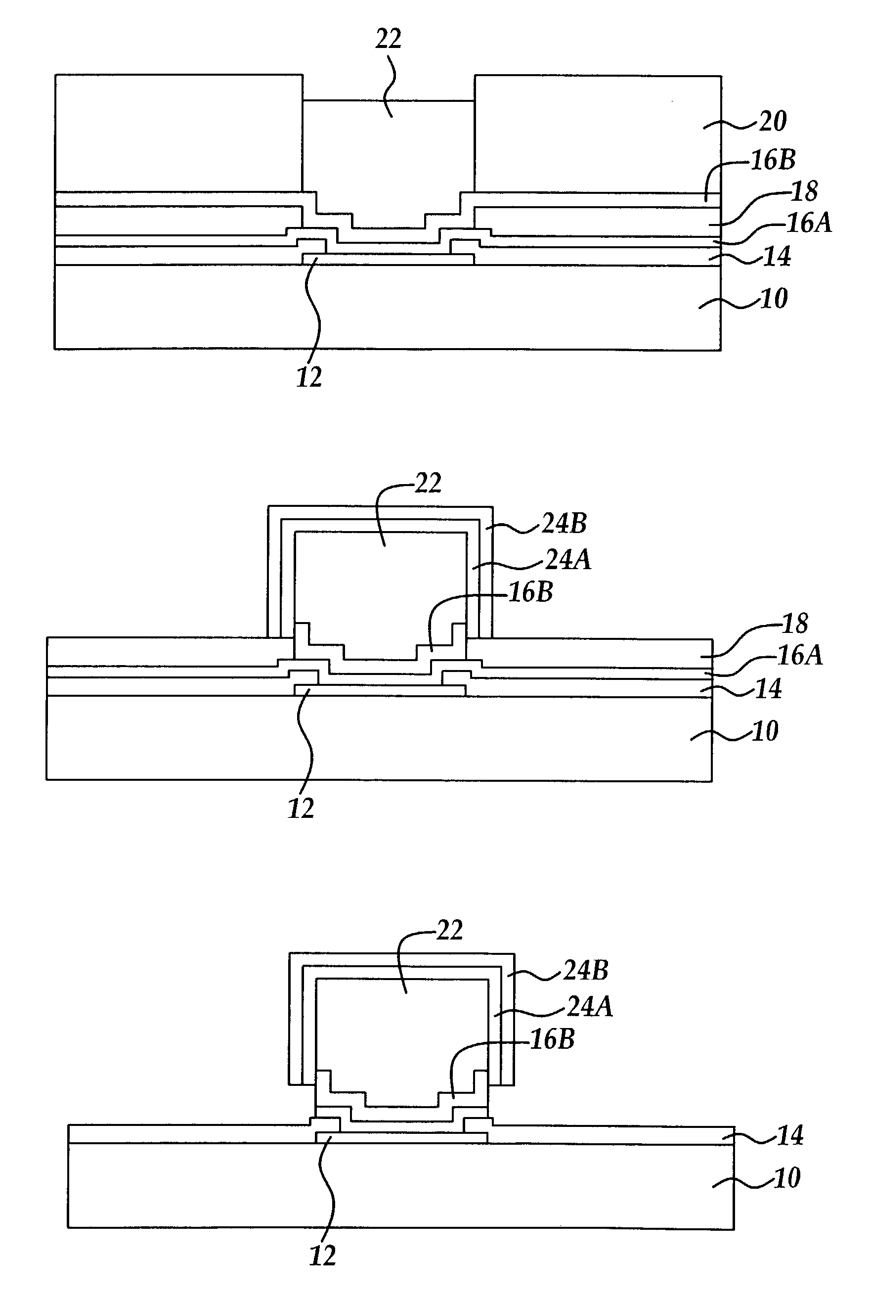
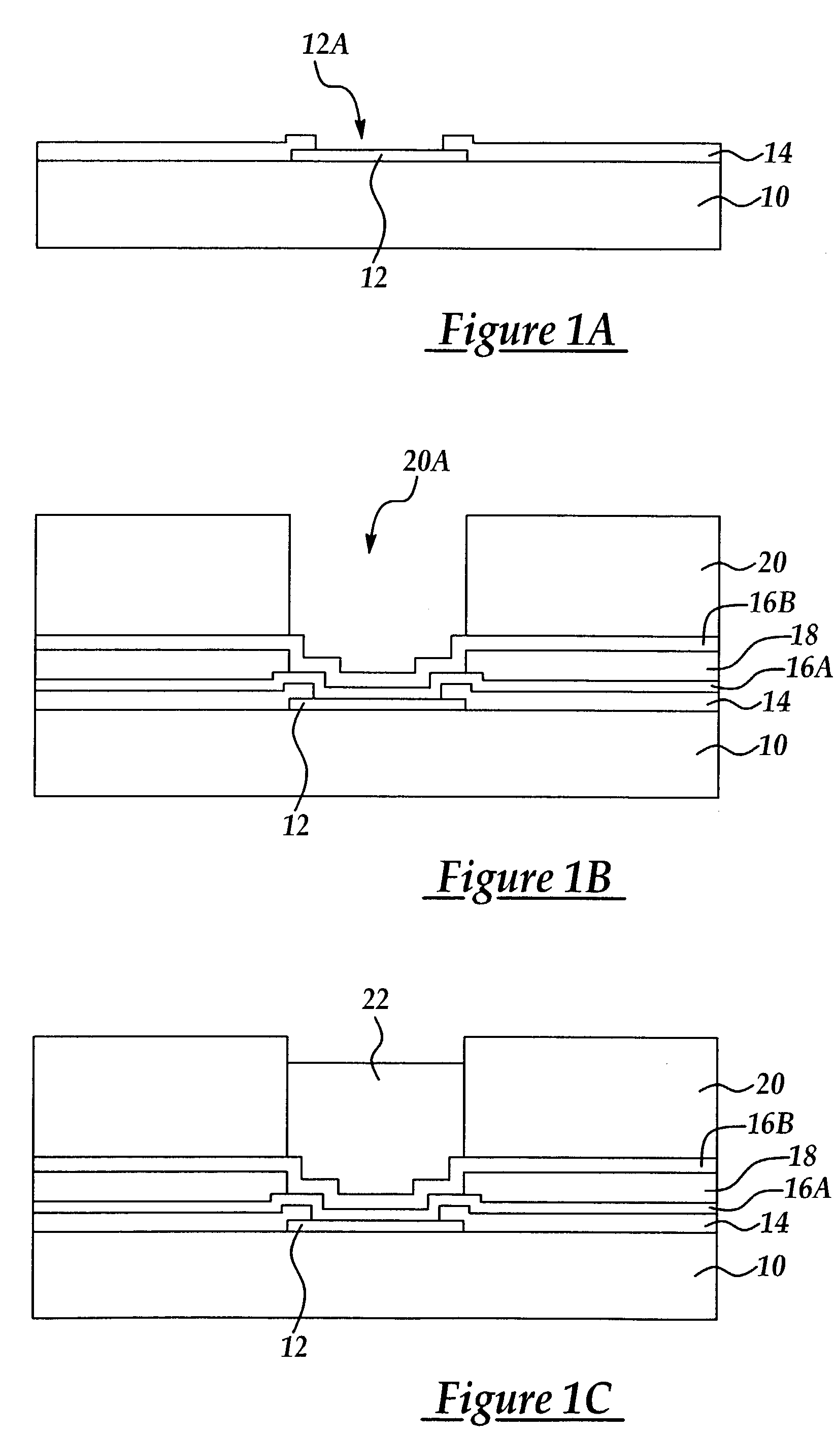
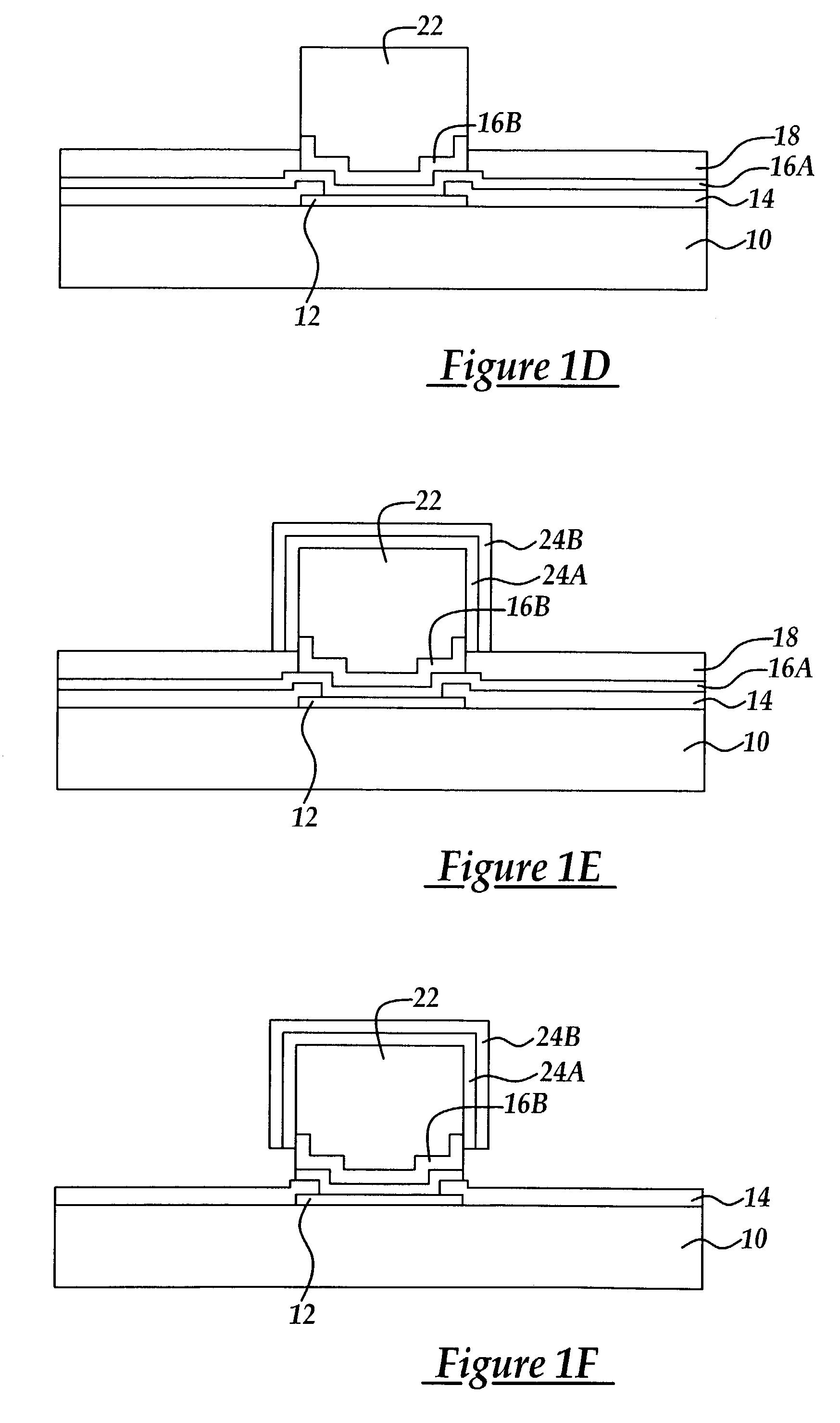
[0015]In an exemplary process for forming a copper bump on a semiconductor chip, reference is made to FIGS. 1A–1F showing representational cross sectional views of a portion of a semiconductor process wafer at exemplary stages in a manufacturing process for forming a copper bump for chip bonding in flip chip bonding technology. By the term “copper” herein in meant copper or alloys thereof. For example, referring first to FIG. 1A, the process of creating the copper bumps begins after chip bonding pad 12, for example Cu or Al, has been formed in an upper portion of an uppermost dielectric insulating layer 10, also referred to as a metallization layer of a multi-layered semiconductor device, for example including alternating layers of metallization layers and dielectric isolation layers formed over a semiconductor substrate. Although not shown, preferably, electrical communication pathways, for example metal interconnect structures such as metal lines or vias are provided in metallizat...


PUM


Abstract

A method for forming a copper bump for flip chip bonding having improved oxidation resistance and thermal stability including providing a copper column having a thickness of at least about 40 microns overlying a metallurgy including an uppermost copper metal layer and a lowermost titanium layer the lowermost titanium layer in contact with an exposed copper bonding pad portion surrounded by a passivation layer; and, selectively depositing at least one protective metal layer over the copper column according to an electrolytic deposition process.

Description

FIELD OF THE INVENTION[0001]This invention generally relates to semiconductor processing and more particularly solder bump formation in flip chip bonding technology and a method for protecting an exposed copper surface in a copper bump from oxidation.BACKGROUND OF THE INVENTION[0002]Packaging of the ULSI chip is one of the most important steps in ULSI manufacturing, contributing significantly to the overall cost, performance and reliability of the packaged chip. As semiconductor devices reach higher levels of integration, packaging technologies such as chip bonding have become critical. Packaging of the chip accounts for a considerable portion of the cost of producing the device and failure of the package leads to costly yield reduction.[0003]Some chip bonding technologies utilize a copper bump attached to a contact pad (chip bond pad) on the chip to make an electrical connection from the chip to the package. For example, new packaging methods including area array mounting include B...

Claims


Application Information

Patent Timeline
IPC IPC(8): H01L21/44H01L21/60H01L23/485
CPCH01L24/03H01L24/05H01L24/11H01L24/12H01L2924/0002H01L2924/01033H01L2924/01024H01L2924/05042H01L2924/014H01L2224/03912H01L2224/0401H01L2224/05562H01L2224/05568H01L2224/05624H01L2224/05647H01L2224/1147H01L2224/11474H01L2224/13023H01L2224/13099H01L2224/13147H01L2924/01004H01L2924/01012H01L2924/01013H01L2924/01014H01L2924/01022H01L2924/01028H01L2924/01029H01L2924/0104H01L2924/01078H01L2924/01079H01L2924/00014H01L2224/05552H01L2224/05556H01L2224/13562H01L2924/00012
Inventor LEI, KUO LUNG
Owner HON HAI PRECISION IND CO LTD
Why Eureka
Try Eureka