Pattern formation method

Inactive Publication Date: 2006-03-14
PANASONIC CORP
View PDF4 Cites 0 Cited by
  • Summary
  • Abstract
  • Description
  • Claims
  • Application Information

AI Technical Summary

Benefits of technology

[0023]In the first or second pattern formation method of this invention, a chemically amplified resist film is formed on the underlying film having two molecular layers, that is, the first and second molecular layers, thereon. Therefore, moisture or an alkaline impurity included in the underlying film is blocked by the two molecular layers and hence minimally reaches the bottom of the resist film. Accordingly, when the resist film is subjected to the pattern exposure, phenomenon that an acid generated from an acid generator is degraded in its acidity by the moisture or is deactivated through neutralization with the alkaline impurity minimally occurs, so that a catalytic reaction of the acid can be sufficiently performed at the bottom of an exposed portion of the resist film. As a result, a resist pattern can be formed in a good cross-sectional shape free from a footing shape or an undercut shape.

Problems solved by technology

As a result, it has been found that in the case where an underlying film has pores or includes an organic material, the shape of a resultant resist pattern formed thereon becomes defective.
Accordingly, the amount of acid is insufficient at the bottom of an exposed portion of the resist film, so that a catalytic reaction of the acid cannot be sufficiently carried out.
As a result, solubility in a developer is spoiled at the bottom of an exposed portion of a negative resist film and insolubility in a developer is spoiled at the bottom of an exposed portion of a positive resist film, and therefore, a positive resist pattern is in a defective footing shape and a negative resist pattern is in a defective undercut shape.

Method used


Image

  • Pattern formation method
  • Pattern formation method
  • Pattern formation method

Examples


embodiment 1

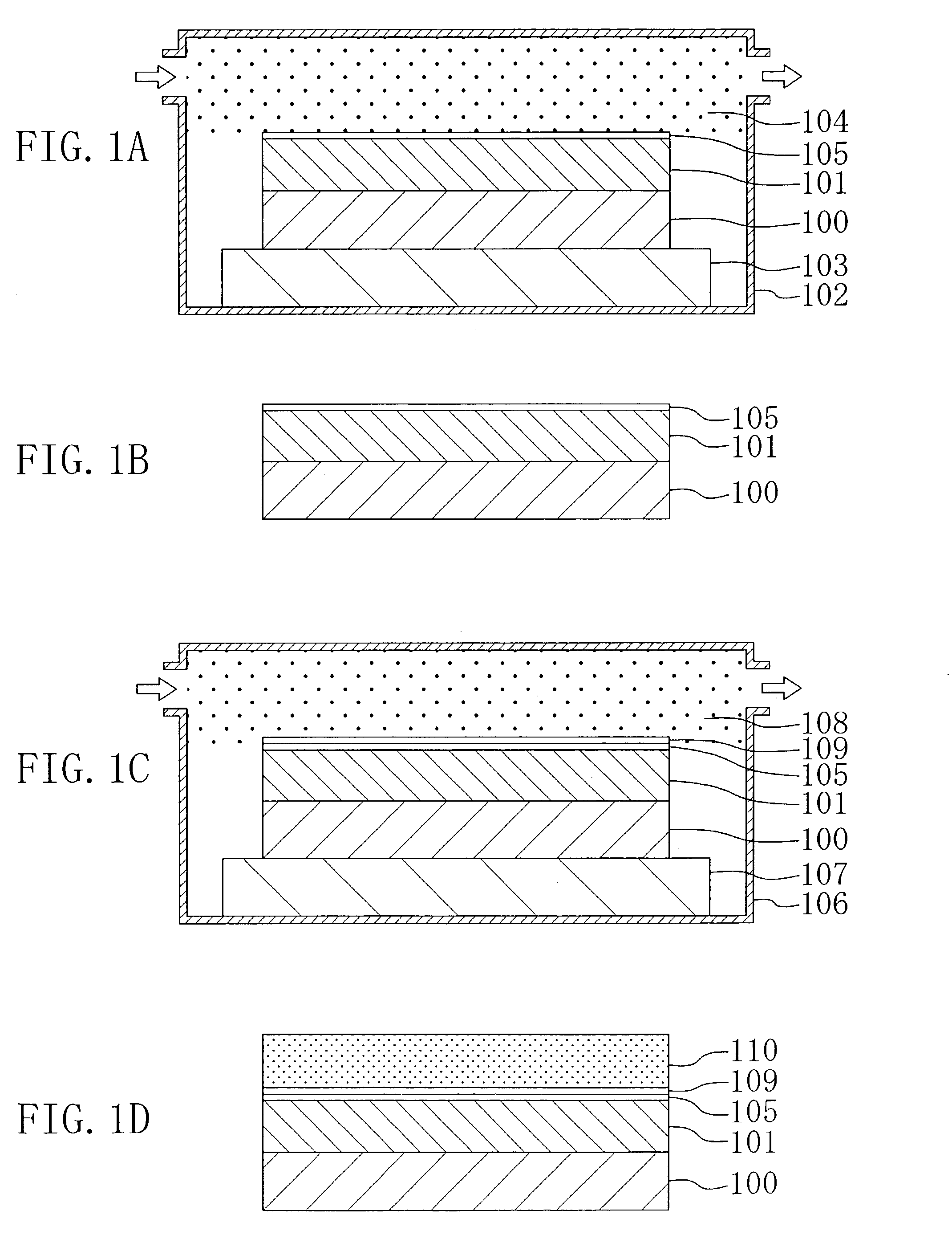
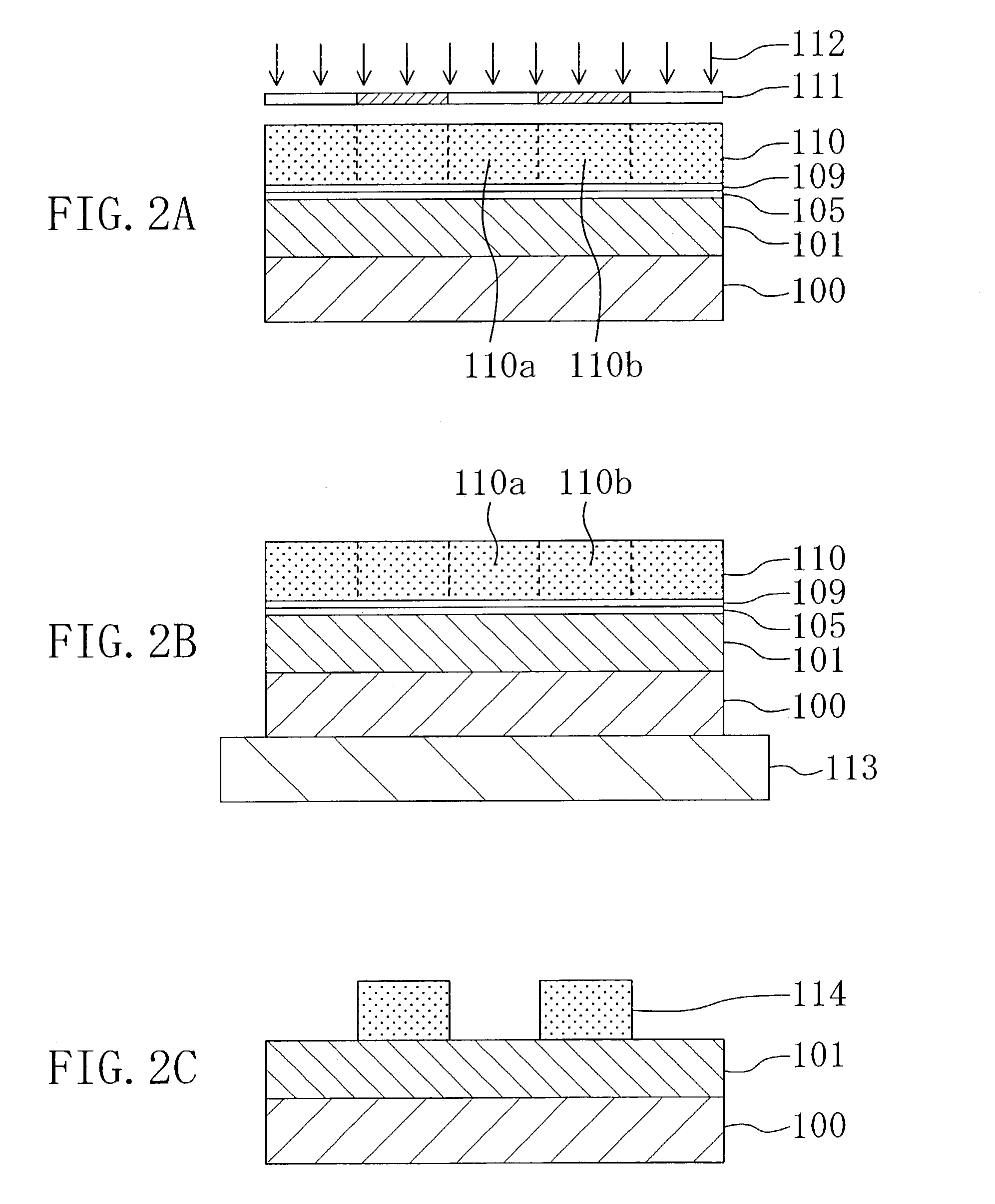
[0035]A pattern formation method according to Embodiment 1 of the invention will now be described with reference to FIGS. 1A through 1D and 2A through 2C.

[0036]First, a chemically amplified resist material having the following composition is prepared:

[0037]

Base polymer: poly((methoxymethyl acrylate) −  2 g(γ-butyrolactone methacrylate))(wherein methoxymethyl acrylate:γ-butyrolactonemethacrylate = 70 mol %:30 mol %)Acid generator: triphenylsulfonium triflate0.04 gSolvent: propylene glycol monomethyl ether acetate  20 g

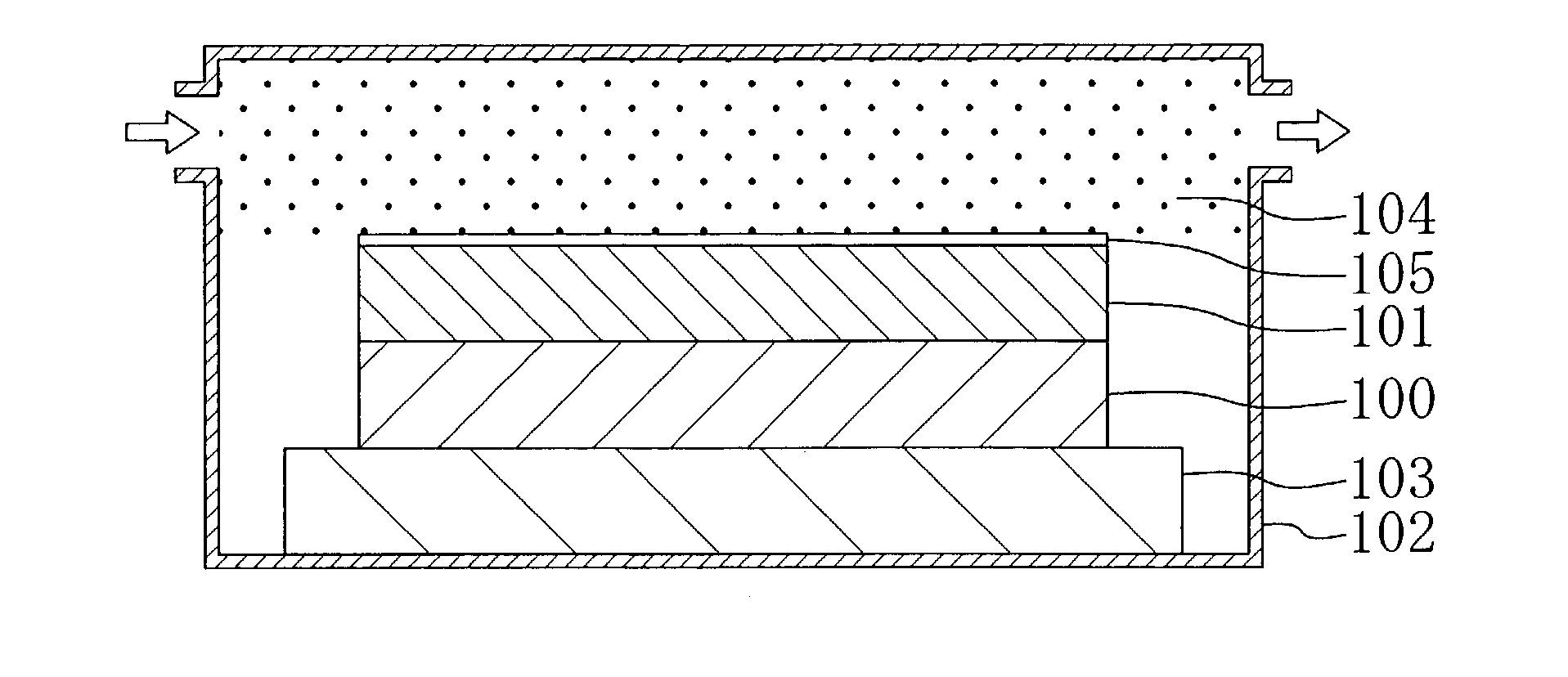
[0038]Next, as shown in FIG. 1A, an organic polymer made of aromatic hydrocarbon including no fluorine (for example, SiLK manufactured by Hitachi Chemical Co., Ltd. (with a dielectric constant of 2.65)) is deposited on a substrate 100, so as to form a low dielectric insulating film 101 corresponding to an underlying film. Thereafter, the substrate 100 is placed in a first chamber 102 and kept on a first hot plate 103. Then, while annealing the substrate 100 with the fir...

embodiment 2

[0049]A pattern formation method according to Embodiment 2 of the invention will now be described with reference to FIGS. 3A through 3D and 4A through 4C.

[0050]First, a chemically amplified resist material having the following composition is prepared:

[0051]

Base polymer: poly((methoxymethyl acrylate) −  2 g(γ-butyrolactone methacrylate))(wherein methoxymethyl acrylate:γ-butyrolactonemethacrylate = 70 mol %:30 mol %)Acid generator: triphenylsulfonium triflate0.04 gSolvent: propylene glycol monomethyl ether acetate  20 g

[0052]Next, as shown in FIG. 3A, an organic polymer made of aromatic hydrocarbon including no fluorine (for example, SiLK manufactured by Hitachi Chemical Co., Ltd. (with a dielectric constant of 2.65)) is deposited on a substrate 200, so as to form a low dielectric insulating film 201 corresponding to an underlying film. Thereafter, the substrate 200 is placed in a chamber 202 and kept on a first hot plate 203. Then, while annealing the substrate 200 with the first hot...

embodiment 3

[0062]A pattern formation method according to Embodiment 3 of the invention will now be described with reference to FIGS. 5A through 5D and 6A through 6C.

[0063]First, a chemically amplified resist material having the following composition is prepared:

[0064]

Base polymer: poly(vinyl phenol)  6 gCrosslinking agent: 2,4,6-tris(methoxymethyl)0.12 gamino-1,3,5-s-triazineAcid generator: phthalimino triflate0.02 gSolvent: propylene glycol monomethyl ether acetate  30 g

[0065]Next, as shown in FIG. 5A, an organic polymer made of aromatic hydrocarbon including no fluorine (for example, SiLK manufactured by Hitachi Chemical Co., Ltd. (with a dielectric constant of 2.65)) is deposited on a substrate 300, so as to form a low dielectric insulating film 301 corresponding to an underlying film. Thereafter, the substrate 300 is placed in a first chamber 302 and kept on a first hot plate 303. Then, while annealing the substrate 300 with the first hot plate 303 at a temperature of 90° C., gas-phase hex...


PUM


Abstract

An underlying film having pores or including an organic material is formed on a substrate. In a first chamber, hexamethyldisilazane is supplied onto the surface of the underlying film while annealing the substrate, so as to form a first molecular layer of trimethylsilyl groups on the underlying film. Thereafter, the underlying film is allowed to stand outside the first chamber. Next, in a second chamber, hexamethyldisilazane is supplied onto the surface of the first molecular layer, so as to form a second molecular layer of trimethylsilyl groups on the first molecular layer. Then, a resist film made of a chemically amplified resist material is formed above the underlying film having the second molecular layer thereon. The resist film is subjected to pattern exposure by selectively irradiating with exposing light, and the resist film is developed after the pattern exposure, so as to form a resist pattern.

Description

BACKGROUND OF THE INVENTION[0001]The present invention relates to a pattern formation method for use in fabrication processing or the like for a semiconductor integrated circuit device.[0002]In the fabrication processing for a semiconductor integrated circuit device, the size of a resist pattern (pattern width) formed by lithography technique is required to be further refined in accordance with increase in the degree of integration of semiconductor integrated circuits.[0003]Also, the dielectric constant of an insulating film is desired to be further lowered in accordance with improved performance of semiconductor devices. Therefore, use of a low dielectric insulating film that has a lower dielectric constant than a generally used silicon oxide film, such as an insulating film having pores or including an organic material, has been proposed.[0004]Now, a conventional pattern formation method will be described with reference to FIGS. 8A through 8C, 9A and 9B.[0005]First, a chemically a...

Claims


Application Information

Patent Timeline
IPC IPC(8): G03F7/00G03F7/038G03F7/039G03F7/075G03F7/11G03F7/16G03F7/38H01L21/027
CPCG03F7/0751G03F7/11G03F7/165G03F7/161
Inventor ENDO, MASAYUKISASAGO, MASARU
Owner PANASONIC CORP
Why Eureka
Try Eureka