Silicon nanotaper couplers and mode-matching devices

a technology of mode-matching devices and nano-taper couplers, which is applied in the direction of optical waveguide light guides, instruments, optics, etc., can solve the problems of limiting the use of nano-taper couplers, utilizing prior art nano-taper couplers, and all of these preparation activities are expensive and time-consuming, so as to reduce reflections, improve efficiency, and reduce the lateral dimension of in-coupled optical beams

Active Publication Date: 2006-03-14
CISCO TECH INC
View PDF9 Cites 42 Cited by
  • Summary
  • Abstract
  • Description
  • Claims
  • Application Information

AI Technical Summary

Benefits of technology

[0013]It is an advantage of the present invention that the utilization of a thin dielectric coupling waveguide with a core refractive index less than silicon allows for various adjustments to be made in the free-space coupling arrangement to provide for improved efficiency. For example, the thickness of the dielectric layer may be controlled by conventional CMOS fabrication processes to provide the optimum thickness required for coupling (as a function of the specific dielectric material selected).
[0014]In a preferred embodiment of the present invention, focusing optics are included within the dielectric coupling waveguide to reduce the lateral dimension of the in-coupled optical beam as it approaches the entrance of the silicon nanotaper. The dielectric coupling waveguide may itself include a tapered profile in the lateral dimension to reduce reflections at the interface with the nanotaper.
[0015]The utilization of a material other than silicon for the dielectric coupling waveguide allows for materials other than silicon to also be used to form the associated free-space optical coupler, providing for some relaxation on the geometry of the launch conditions required for coupling a light beam into and out of a surface waveguide layer.
[0016]It is an aspect of the present invention that the dielectric coupling waveguide in conjunction with a silicon nanotaper may be used to provide coupling into and out of ultrathin silicon waveguides at any location on an opto-electronic structure (not limited, that is, for use as an input / output coupler). In this case, the dielectric coupling waveguide can be used to form various optical devices (passive devices) that are not compatible with the properties of ultrathin waveguides (scattering loss problems, for example), reserving the use of the ultrathin waveguides for high-performance active optical devices.

Problems solved by technology

While these and other prior art nanotaper couplers have been successful in bringing light from an optical fiber into an ultrathin single-mode waveguide, there are limitations in how they may be employed.
Perhaps the greatest hindrance in utilizing the prior art nanotaper couplers is the “end fire” coupling requirement; that is, an optical fiber (or other waveguide) must provide a signal that couples through a sidewall (endface) of an optical substrate and into the nanotaper.
All of these preparation activities are expensive and time-consuming.
A larger problem associated with the “end fire” coupling is the fact that only the edge of the substrate may be used for coupling; the remainder of the wafer surface is unavailable for use with a conventional nanotaper coupler.
Additionally, the larger auxiliary waveguide section often requires the use of material several microns thick (in order to establish a low-loss interface to the fiber), where these dimensions are not compatible with conventional CMOS processing techniques.

Method used


Image

  • Silicon nanotaper couplers and mode-matching devices
  • Silicon nanotaper couplers and mode-matching devices
  • Silicon nanotaper couplers and mode-matching devices

Examples


Embodiment Construction

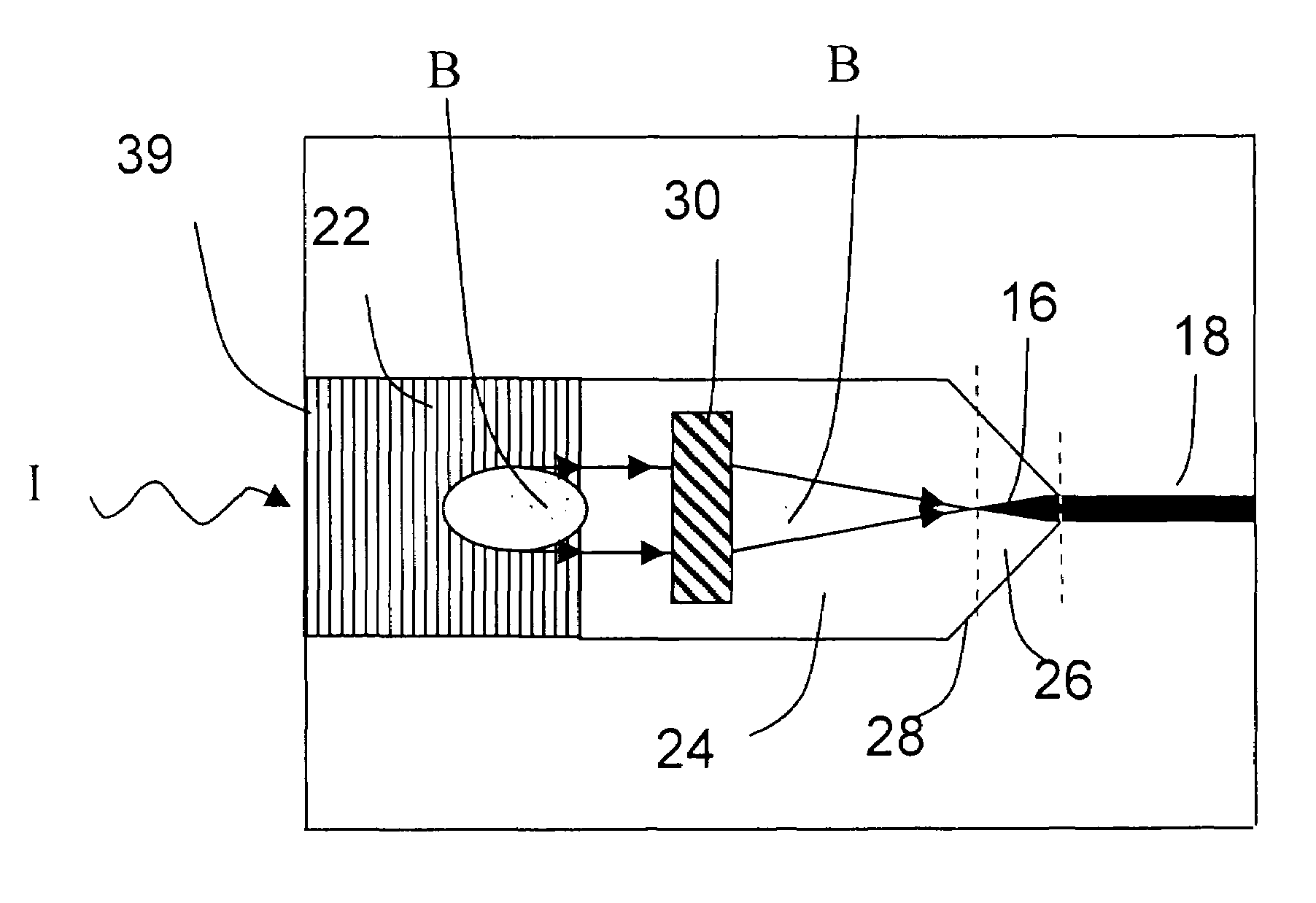
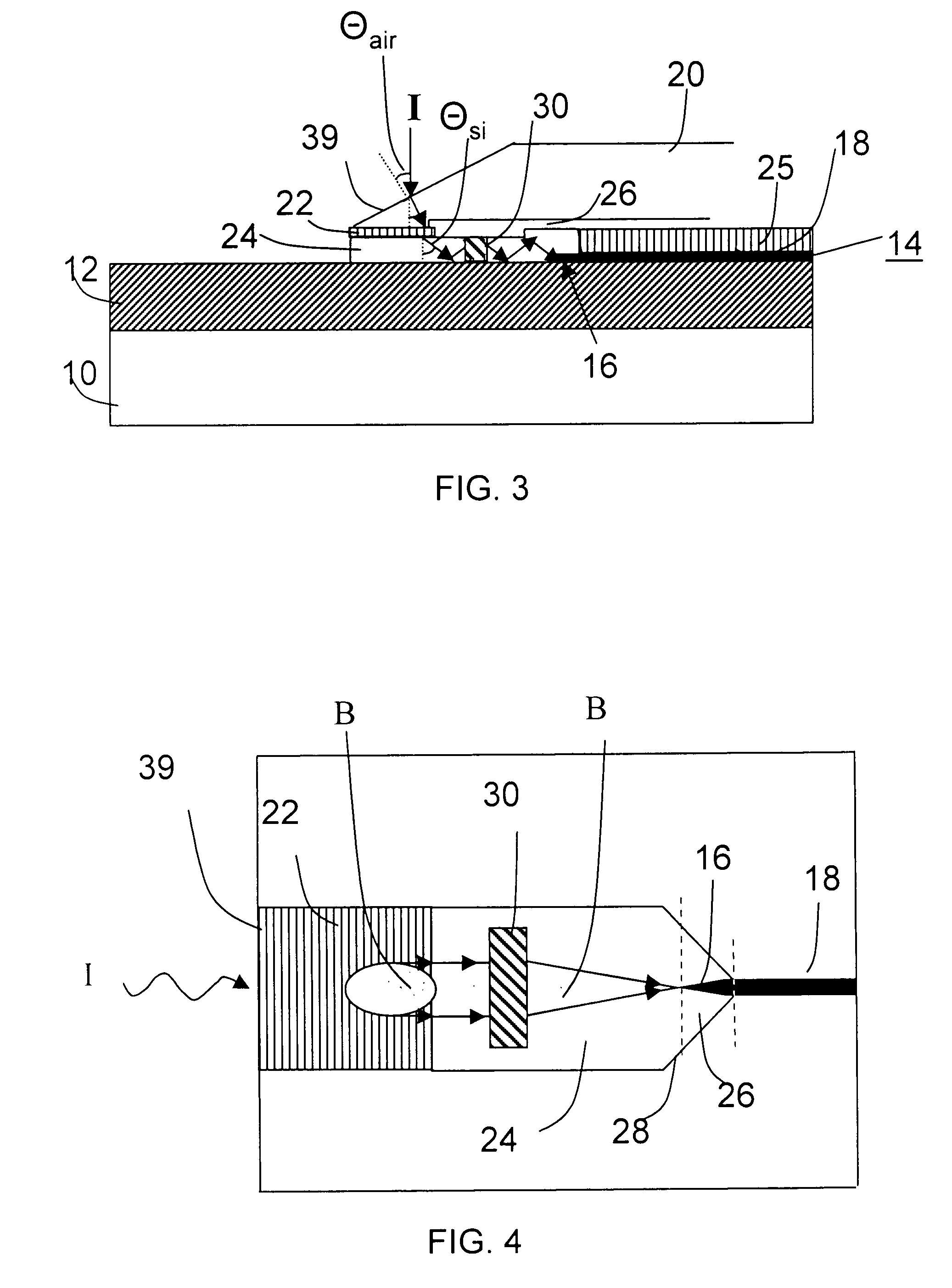
[0032]The utilization of a hybrid coupling arrangement comprising a silicon-based nanotaper coupler and free-space optical coupler, in accordance with the present invention, addresses many of the problems associated with the prior art end-fire couplers and offers additional flexibility with respect to wafer-scale fabrication and free-space optical coupling. FIG. 3 contains a side view, and FIG. 4 a top view, of an SOI-based exemplary hybrid coupler formed in accordance with the present invention. In most cases, the devices formed in accordance with the present invention will comprise an SOI structure including a silicon substrate 10, a silicon dioxide insulating layer 12 and an upper silicon device layer (hereinafter referred to as an “SOI layer”) 14, where SOI layer 14 generally comprises a thickness of less than one micron.

[0033]A silicon nanotaper 16 (best illustrated in FIG. 4) is formed within a portion of SOI layer 14 and used, as discussed above, to provide efficient coupling...


PUM


Abstract

An arrangement for coupling between a free-space propagating optical signal and an ultrathin silicon waveguide formed in an upper silicon layer (SOI layer) of a silicon-an-insulator (SOI) structure includes a silicon nanotaper structure formed in the (SOI layer) and coupled to the ultrathin silicon waveguide. A dielectric waveguide coupling layer is disposed so as to overly a portion of a dielectric insulating layer in a region where an associated portion of the SOI layer has been removed. An end portion of the dielectric waveguide coupling layer is disposed to overlap an end section of the silicon nanotaper to form a mode conversion region between the free-space signal and the ultrathin silicon waveguide. A free-space optical coupling arrangement is disposed over the dielectric waveguide coupling layer and used to couple between free space and the dielectric waveguide coupling layer and thereafter into the ultrathin silicon waveguide.

Description

CROSS-REFERENCE TO RELATED APPLICATION[0001]This application claims the benefit of Provisional Application No. 60 / 543,613, filed Feb. 11, 2004.TECHNICAL FIELD[0002]The present invention relates to silicon-based nanotaper couplers and, more particularly, to nanotaper couplers that may be utilized in conjunction with free-space optical couplers to facilitate the coupling of optical signals into and out of ultrathin, single-mode silicon waveguides.BACKGROUND OF THE INVENTION[0003]A “nanotaper”, or “inverse taper”, is generally defined as a terminating portion of a core of a high-contrast index waveguide that is used to facilitate efficient coupling between a single-mode optical fiber (for example) and an ultrathin, single-mode high-contrast index optical waveguide. For the purposes of the present invention, an “ultrathin” waveguide is defined as having a typical width on the order of approximately 0.5 μm and a typical thickness on the order of approximately 0.25 μm. In a typical device...

Claims


Application Information

Patent Timeline
Patent Type & Authority Patents(United States)
IPC IPC(8): G02B6/26G02B6/122G02B6/14G02B6/34G02B6/42
CPCG02B6/4204G02B6/1228G02B6/14G02B6/26B82Y40/00
Inventor GHIRON, MARGARETGOTHOSKAR, PRAKASHMONTGOMERY, ROBERT KEITHPATEL, VIPULKUMARPATHAK, SOHAMSHASTRI, KALPENDUYANUSHEFSKI, KATHERINE A.
Owner CISCO TECH INC
Why Eureka
Try Eureka