Semiconductor light emitting device and method

a semiconductor and light-emitting technology, applied in the direction of semiconductor devices, basic electric elements, electrical appliances, etc., can solve the problems of absorbing a significant amount of light, reducing the fraction of light that exits the device, and wasting time and energy in prior art approaches to maximize light, etc., to achieve high light generating capability, low series resistance, and high reflective

Inactive Publication Date: 2006-03-21
LUMILEDS
View PDF15 Cites 16 Cited by
  • Summary
  • Abstract
  • Description
  • Claims
  • Application Information

AI Technical Summary

Benefits of technology

[0014]In our above-referenced copending parent applications (Ser. Nos. 09 / 469,657 and 09 / 470,540), there is disclosed a III-nitride semiconductor light-emitting device with an increased light generating capability. In an embodiment thereof, a large area (greater than 400×400 um2) device, formed on a silicon carbide substrate, has an inverted configuration; that is, an epitaxy-side down structure with the light emitted predominately through the substrate. At least one n-electrode interposes the p-electrode metallization to provide low series resistance. The p-electrode metallization is opaque, highly reflective, and Ohmic, and provides excellent current spreading. Light absorption in the p-electrode at the peak emission wavelength of the LED active region is less than 25% per pass. An intermediate material or submount can be used to provide electrical and thermal connection between the LED die and the package. The submount material may be Si to provide electronic functionality such as voltage-compliance limiting operation, protection from electrostatic discharge (ESD), series-string LED arrays, and feedback-controlled light output. The entire device, including the LED-submount interface, is designed for low thermal resistance to allow for high current density operation.
[0015]An approach hereof to fabricating efficient, low-cost small-area surface-mount LED chips employs a substantially transparent, high-refractive index substrate, that can be diced into small chips. One embodiment hereof employs a low light absorption SiC substrate as an extraction window rather than as a conductive substrate. In this embodiment, both p and n contacts are formed on one surface of the LED, facilitating surface-mount attach. Also, the high refractive index of the SiC substrate (n˜2.7) eliminates the waveguide problem imposed by the use of sapphire, resulting in higher extraction efficiency. SiC can be easily diced into very small chips, so efficient low-cost manufacture of small devices is facilitated by the present invention.
[0018]In accordance with a form of the technique of the invention, there is disclosed a method for making semiconductor light emitting device chips, comprising the following steps: providing a substrate of substantially transparent silicon carbide; forming a semiconductor structure on one side of the substrate, the semiconductor structure having a plurality of semiconductor layers and an active region within the layers; applying electrodes to semiconductor layers of the structure to form semiconductor light emitting devices; and dicing the substrate and devices into a plurality of chips. In an embodiment of this form of the invention, the step of forming a semiconductor structure having a plurality of layers comprises providing a plurality of layers including an n-type layer of a III-nitride semiconductor and a p-type layer of a III-nitride semiconductor on opposing sides of the active region. In this embodiment the substrate and devices are sawed into dice of dimensions less than 400×400 um (and / or area less than 0.16 mm2). In a further embodiment, the substrate and devices are sawed into dice of dimensions less than 300×300 um (and / or an area less than 0.09 mm2). Alternatively, in these embodiments, at least one dimension is less than 400 um or 300 um, as the case may be. The silicon carbide substrates are particularly advantageous for this purpose, as compared, for example, to the more common sapphire substrates which cannot be easily diced into such small pieces using presently available techniques without unacceptable breakage that substantially lowers yields.

Problems solved by technology

As noted in the referenced EP Patent Publication, considerable effort has been expended in prior art approaches to maximize the light that is generated from the active region.
Although this increase in size of the p-electrode may increase the amount of light available from the active region, it can decrease the fraction of light that exits the device, since much of the light must pass through the p-electrode.
The transmittance of the p-electrode can be increased by making the electrode thin or providing it with apertures (see, for example copending U.S. patent application Ser. No. 09 / 151,554, filed Sep. 11, 1998), but even these somewhat transmissive electrodes can absorb a significant amount of light, and their light transmission characteristics tend to trade-off against electrical operating efficiency, such as by compromising the uniform current density desired for the active region.
The most common substrate is sapphire, but the relatively low refractive index of sapphire (n˜1.8) limits performance due to index mismatch with the epitaxial region (which has n˜2.4) that results in a “waveguiding” effect on some of the light generated at the active region.
Roughening of the sapphire / epilayer interface can help somewhat, but is of limited effectiveness and can have other disadvantages.
All of these approaches tend to be performance limited by, inter alia, the above-noted effect of a portion of the light being waveguided and trapped because of the sapphire / epitaxy index mismatch.
The growth conditions required for a conductive buffer layer limits the growth conditions available for subsequent layers and thus restricts the quality of the III-nitride active region layers.
Also, the conductive buffer layer may introduce optical loss mechanisms that limit light extraction efficiency.
Optical absorption resulting from SiC substrate dopants limits the light extraction efficiency of the device.
These conditions result in a trade-off between series resistance and light extraction efficiency and serve to limit the electrical-to-optical power conversion efficiency of the LED.
However, in addition to the previously mentioned problem of light loss due to waveguiding, the sapphire substrate is difficult to dice in sizes less than 400×400 um^2, making it difficult to fabricate low-cost surface mount LED chip devices.
Scribing-and-breaking, or sawing, the sapphire at these dimensions results in undesirably low yields and is unfavorable for high-volume manufacturing.
A disadvantage is that the vertical-injection device is more difficult to package in a surface mount fashion since p and n contacts are on opposing surfaces, and wirebonds onto the LED chip are required.
Furthermore, as previously noted, the doping required for SiC to be conducting results in excessive light absorption within the chip and limits extraction efficiency.
Accordingly, conductive silicon carbide substrates do not offer a viable approach for manufacture of devices such as III-nitride small-area surface-mount LED chips.

Method used


Image

  • Semiconductor light emitting device and method
  • Semiconductor light emitting device and method
  • Semiconductor light emitting device and method

Examples


Embodiment Construction

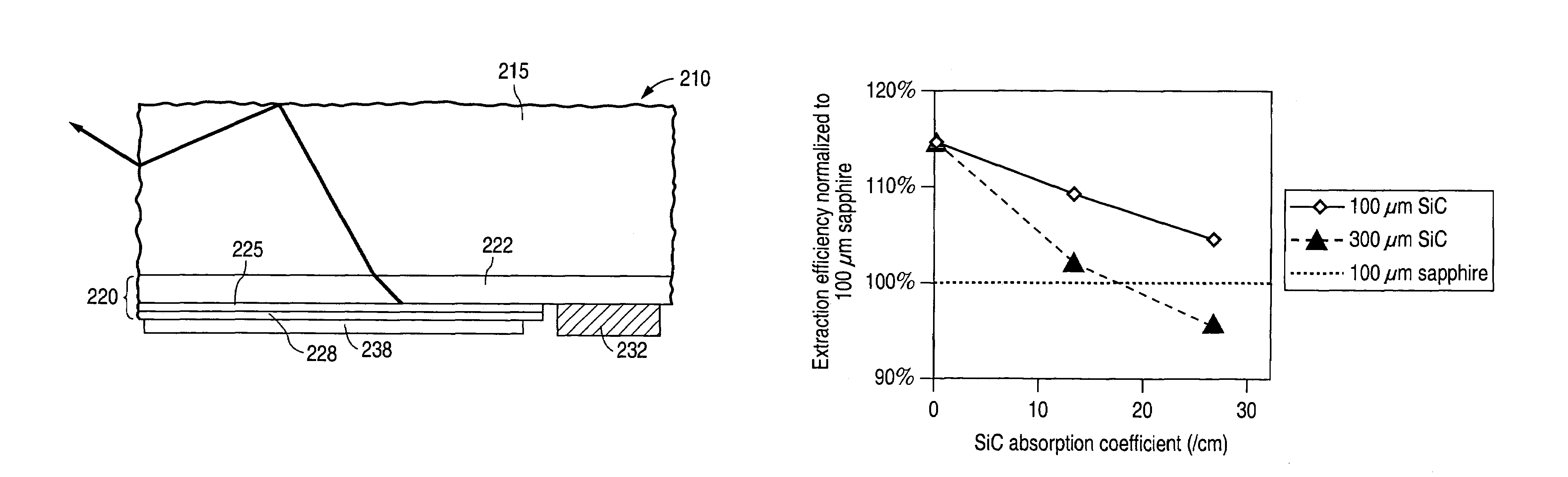
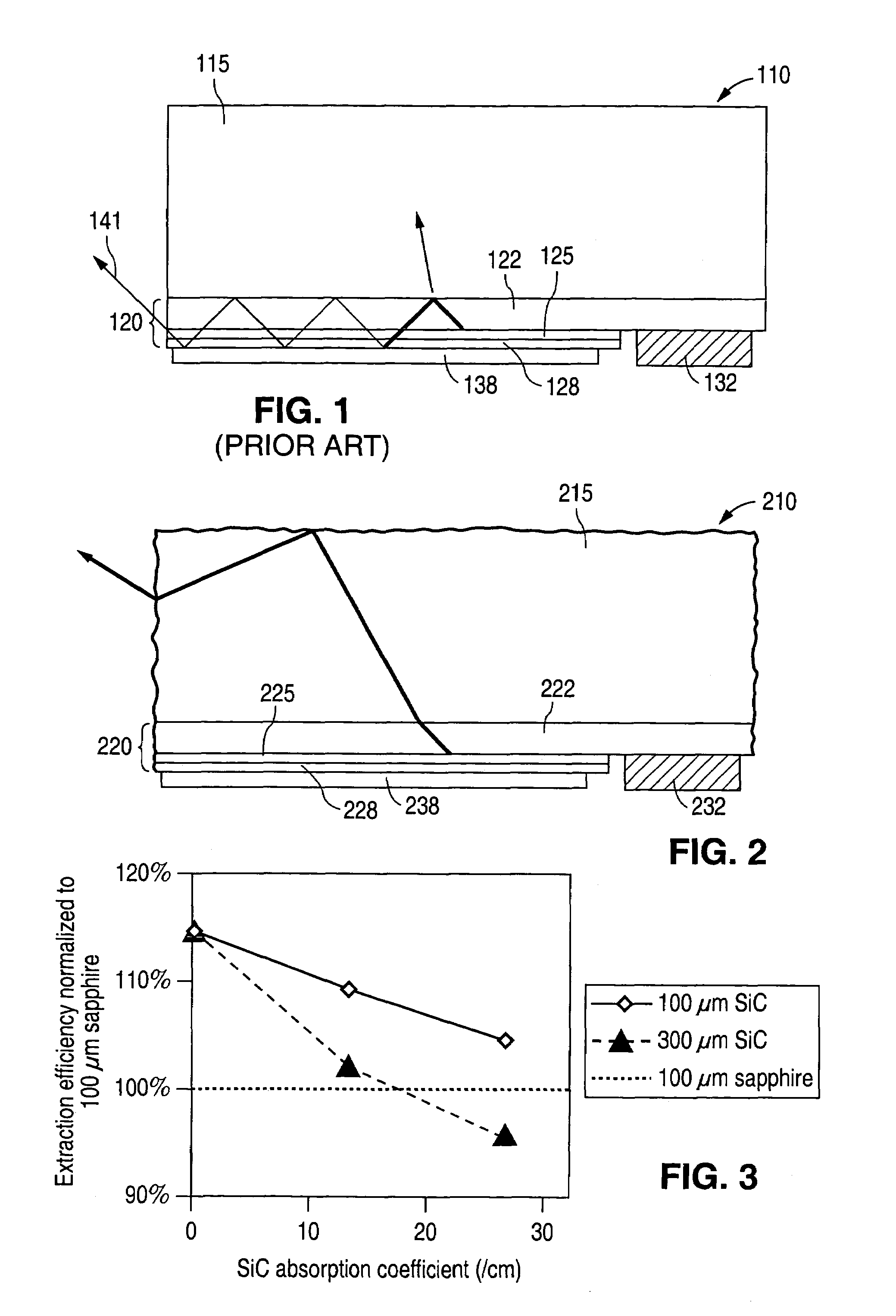
[0024]FIG. 1 illustrates an example of a prior art type of III-nitride semiconductor device 110 in a so-called flip-chip or inverted or epitaxy-down configuration. In this example, the substrate 115, on which the device was originally formed, is sapphire, which has an index of refraction n˜1.8. [The substrate 115, after inversion, is sometimes referred to as a superstrate.] The epitaxy region 120 of III-nitride semiconductor layers includes n-type layer 122 and p-type layer 128, with an active region p-n junction between the n-type and p-type layers. Typically, an active region layer 125 of III-nitride semiconductor is disposed at the p-n junction. A conductive p-electrode 138 is deposited on the p-type layer 128 and a conductive n-electrode 132 is deposited on the n-type layer 122. In this prior art configuration, the electrodes are typically opaque and reflective, and the objective is to emit as much of the light as possible through the top and sides of the sapphire superstrate 11...


PUM

PropertyMeasurementUnit
thicknessaaaaaaaaaa
thicknessaaaaaaaaaa
areaaaaaaaaaaa

Abstract

A light-emitting device includes: a semiconductor structure formed on one side of a substrate, the semiconductor structure having a plurality of semiconductor layers and an active region within the layers; and first and second conductive electrodes contacting respectively different semiconductor layers of the structure; the substrate comprising a material having a refractive index n>2.0 and light absorption coefficient α, at the emission wavelength of the active region, of α>3 cm−1. In a preferred embodiment, the substrate material has a refractive index n>2.3, and the light absorption coefficient, α, of the substrate material is α<1 cm−1.

Description

[0001]This application is a division of application Ser. No. 09 / 803,002 filed Mar. 9, 2001, now U.S. Pat. No. 6,646,292, incorporated herein by reference, which is a continuation-in-part of U.S. patent application Ser. No. 09 / 469,657, now U.S. Pat. No. 6,486,499, and of U.S. patent application Ser. No. 09 / 470,540, now U.S. Pat. No. 6,473,885, both filed on Dec. 22, 1999, and both assigned to the same assignee as the present application.FIELD OF THE INVENTION[0002]This invention relates to light emitting semiconductor structures and methods of making same and, more particularly, to devices and methods employing group III–V nitride semiconductors and to improving the manufacture and the operation thereof.BACKGROUND OF THE INVENTION[0003]Light emitting semiconductors which emit in several regions of the visible spectrum, for example group III–V semiconductors such as aluminum gallium arsenide and gallium phosphide, have achieved commercial acceptance for various applications. However, ...

Claims


Application Information

Patent Timeline
Patent Type & Authority Patents(United States)
IPC IPC(8): H01L21/00H01L27/15H01L33/02H01L33/22H01L33/38H01L33/40H01L33/64
CPCH01L33/22H01L27/156H01L33/02H01L33/025H01L33/38H01L33/40H01L33/405H01L33/64H01L33/641
Inventor STEIGERWALD, DANIEL A.KRAMES, MICHAEL R.
Owner LUMILEDS
Why Eureka
Try Eureka