High resistivity silicon carbide single crystal

a silicon carbide, single crystal technology, applied in the direction of crystal growth process, basic electric elements, electrical equipment, etc., can solve the problems of deterioration of crystal quality, lower crystal growth yield, detrimental side effects, etc., and achieve high resistivity and stable and linear characteristics.

Inactive Publication Date: 2006-03-28
OKMETIC OY
View PDF2 Cites 19 Cited by
  • Summary
  • Abstract
  • Description
  • Claims
  • Application Information

AI Technical Summary

Benefits of technology

[0012]The purpose of the invention is to provide a high resistivity silicon carbide substrate with electrical properties and structural quality suitable for subsequent device manufacturing, such as for example SiC or nitride based high frequency devices, so that the devices can exhibit stable and linear characteristics.
[0013]Another purpose of the invention is to provide a high resistivity silicon carbide substrate having a low density of structural defects and a substantially controlled uniform radial distribution of its resistivity.
[0015]It is a still further purpose of the invention to provide a method for reproducibly controlling the resistivity of the substrate by controlling the type of electrically active intrinsic defects introduced into the crystal during the growth process.

Problems solved by technology

SiC devices with power densities exceeding those of GaAs and Si LDMOS technologies have been realized, however, there are still a number of issues that need to be addressed in order to realize the full potential of SiC based microwave technologies.
Semi-insulating SiC substrates can also have a higher micropipe density than conductive substrates and tend to suffer lower crystal growth yields.
It is now quite well established that producing semi-insulating silicon carbide crystal by vanadium doping can in certain practical situations lead to detrimental side effects such as a deterioration of the crystal quality and low process yields.
However, certain intrinsic defects can be thermally unstable and if used in a semi-insulating silicon carbide substrate, the resistivity of the substrate may not be well controlled under certain conditions.
This effect deteriorates the device characteristics, as the device is unstable and has a power handling capability lower than what it is designed for.

Method used


Image

  • High resistivity silicon carbide single crystal
  • High resistivity silicon carbide single crystal
  • High resistivity silicon carbide single crystal

Examples


Embodiment Construction

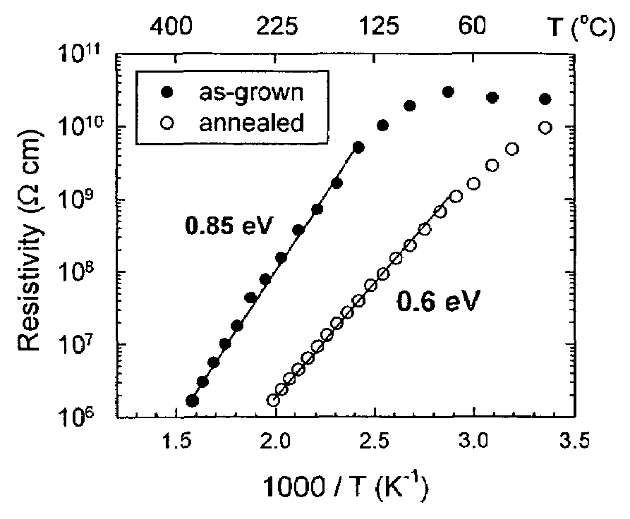
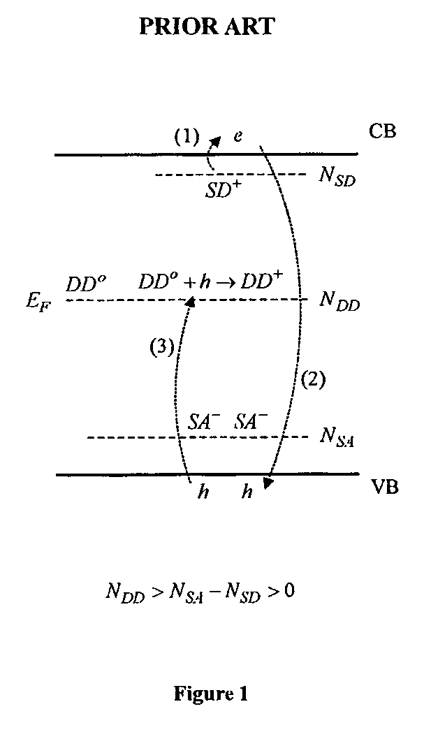
[0034]The presence of trap related drain current collapse in SiC MESFETs and the higher micropipe density often encountered in vanadium doped substrates motivate the development of high-resistivity substrates with a controlled composition minimizing the concentration of detrimental traps.

[0035]This requires crystal growth processes using a pure growth environment. In the High Temperature Chemical Vapour Deposition (HTCVD) technique, where the source material is in-situ synthesised from purified gas precursors, the gas phase composition can be controlled to either decrease the incorporation of undesirable impurities or, as it will be shown, to promote the incorporation of specific extrinsic and intrinsic defects. At the same time, the composition of the crystal needs to be controlled to provide the necessary mechanisms to maintain its resistivity at a value useful for microwave device applications.

[0036]The basic method to grow a high resistivity crystal, which applies to silicon car...


PUM

PropertyMeasurementUnit
resistivityaaaaaaaaaa
temperaturesaaaaaaaaaa

Abstract

The purpose of the invention is to provide a high resistivity silicon carbide substrate with electrical properties and structural quality suitable for subsequent device manufacturing, such as for example high frequency devices, so that the devices can exhibit stable and linear characteristics and to provide a high resistivity silicon carbide substrate having a low density of structural defects and a substantially controlled uniform radial distribution of its resistivity.

Description

BACKGROUND OF THE INVENTION[0001]1. Field of the Invention[0002]The present invention relates to a high resistivity silicon carbide single crystal from which substrates for the processing of high frequency semiconductor devices such as MESFETs can be made. The composition of the high resistivity substrates is chosen so that trapping effects deteriorating the performances of the devices are eliminated. The invention also relates to silicon carbide substrates which have a high resistivity before being processed and are able to maintain a high resistivity after processing steps involving heating at temperatures above 1500° C.[0003]2. Background and Prior Art[0004]Semi-insulating, or high resistivity, silicon carbide (SiC) substrates are required for the fabrication of SiC and III-N power microwave devices with low RF losses. SiC devices with power densities exceeding those of GaAs and Si LDMOS technologies have been realized, however, there are still a number of issues that need to be ...

Claims


Application Information

Patent Timeline
Patent Type & Authority Patents(United States)
IPC IPC(8): C30B29/36C30B25/00H01L21/04H01L21/205
CPCC30B25/00H01L21/0445C30B29/36
Inventor ELLISON, ALEXANDRESON, NGUYEN TIENMAGNUSSON, BJORNJANZEN, ERIK
Owner OKMETIC OY
Why Eureka
Try Eureka