Vacuum chuck utilizing sintered material and method of providing thereof

Inactive Publication Date: 2006-04-04
TOKYO ELECTRON LTD
View PDF239 Cites 24 Cited by
  • Summary
  • Abstract
  • Description
  • Claims
  • Application Information

AI Technical Summary

Benefits of technology

[0010]One aspect of the invention is directed to a vacuum chuck for holding a semiconductor wafer during high pressure processing. The vacuum chuck comprises a semiconductor holding region for holding the semiconductor wafer. The vacuum chuck includes a vacuum port for applying vacuum to a surface of the semiconductor wafer. The vacuum chuck includes a material that is applied between the surface of the semiconductor wafer and the semiconductor holding region. The material, preferably a sintered material, is configurable to provide a uniform surface between the surface of the semiconductor wafer and the semiconductor holding region. The vacuum chuck further includes a vacuum region, such as vacuum groove, coupled to the vacuum port. The vacuum groove alternatively has a tapered configuration. The vacuum region is positioned to apply the vacuum to the surface of the semiconductor wafer. The semiconductor holding region has a smooth surface.
[0011]In yet another aspect, the invention is directed to a vacuum chuck for holding a semiconductor wafer during high pressure processing. The vacuum chuck comprises a semiconductor wafer holding region and a vacuum region that is located within the holding region. The vacuum region applies vacuum to a surface of the semiconductor wafer. A sintered material is applied between the surface and the vacuum region, wherein the sintered material relieves stress that is applied by the vacuum. The vacuum region comprises one or more vacuum grooves, whereby the one or more vacuum grooves alternatively have a tapered configuration. The vacuum chuck fu

Problems solved by technology

Processing of semiconductor substrates or wafers presents unique problems not associated with processing of other workpieces.
However, recent advancements for the integrated circuits have made the plasma ashing and the stripper bath untenable for highly advanced integrated circuits.
The small critical dimensions for the etch features result in insufficient structure for lines to withstand the stripper bath leading to a need for a replacement for the stripper bath.
Many of the low dielectric constant materials cannot withstand an oxygen environment of the plasma ashing leading to a need for a replacement for the plasma ashing.
High pressure processing chambers of existing supercritical processing systems are not appropriate to meet the unique needs of the semiconductor processin

Method used


Image

  • Vacuum chuck utilizing sintered material and method of providing thereof
  • Vacuum chuck utilizing sintered material and method of providing thereof
  • Vacuum chuck utilizing sintered material and method of providing thereof

Examples


Example

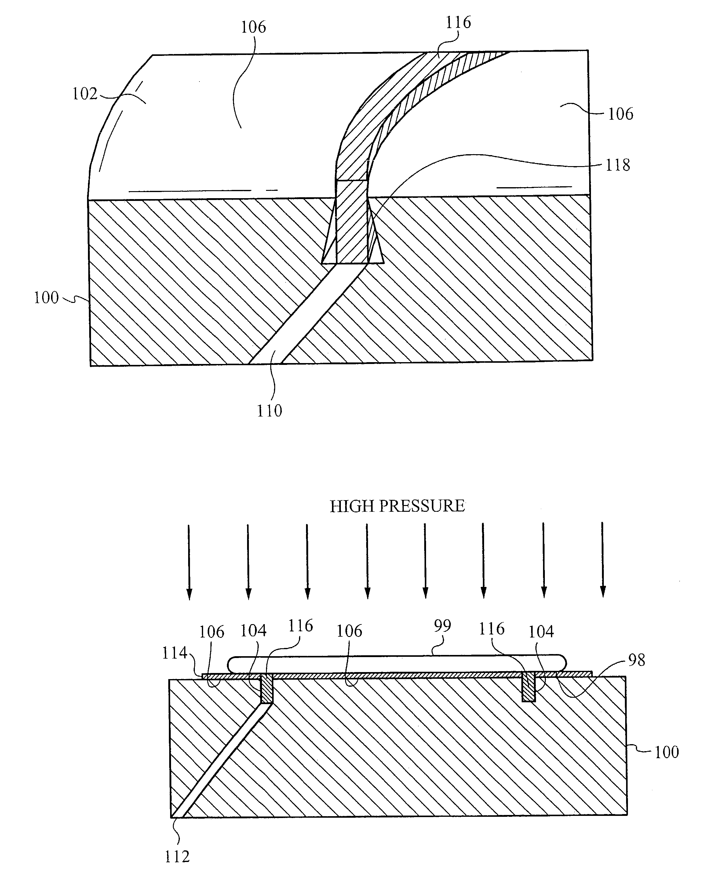
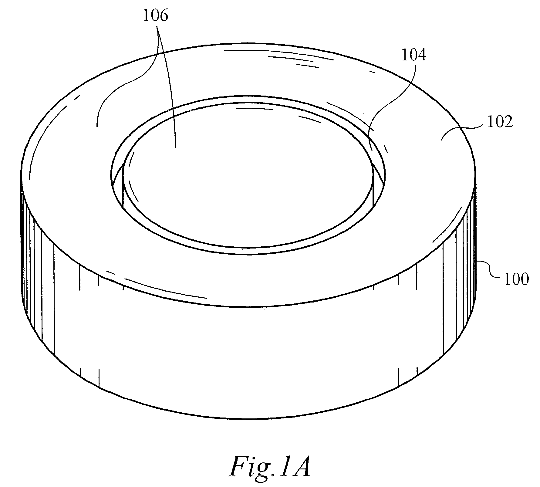
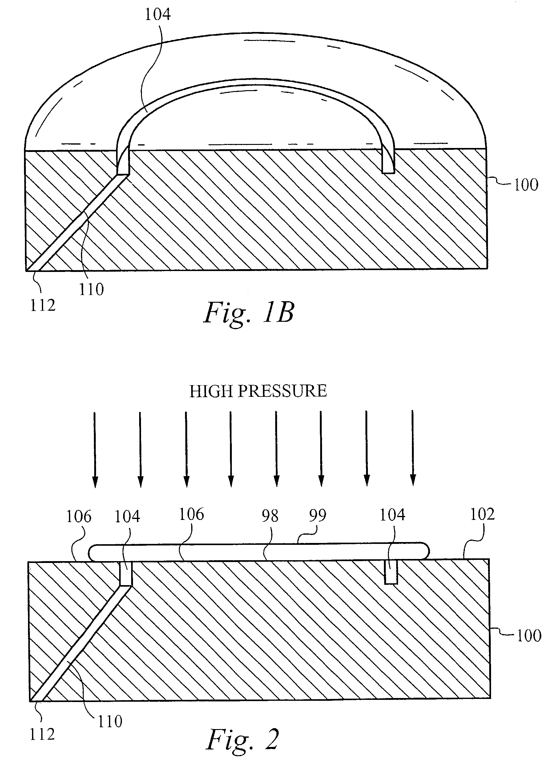
[0022]The preferred vacuum chuck of the present invention preferably holds a semiconductor wafer in a pressure chamber during high pressure, preferably supercritical, processing. FIG. 1A illustrates a perspective view of a vacuum chuck 100 used with the methods in accordance with the present invention. The vacuum chuck 100 is shown having a circular configuration. Alternatively, the vacuum chuck 100 has other shaped configurations, including, but not limited to square or rectangular shapes. The vacuum chuck 100 is preferably a single piece, as shown in FIG. 1A. Alternatively, the vacuum chuck 100 is an assembly of several parts or part of a chamber wall (not shown). The vacuum chuck 100 includes a wafer platen 102 shown at the top surface of the chuck 100. The wafer platen 102 includes a vacuum region 104 and a semiconductor holding region 106. The holding region 106 includes the area of the wafer platen 102 on top of which the semiconductor wafer (not shown) is placed. The holding ...


PUM


Abstract

A vacuum chuck for holding a semiconductor wafer during high pressure, preferably supercritical, processing comprising: a wafer holding region for holding the wafer; a vacuum region for applying vacuum to a surface of the wafer, the vacuum region within the wafer holding region; and a material, preferably sintered material, applied within the vacuum region, the material configurable to provide a uniform surface between the surface of the wafer and the wafer holding region, wherein the material is configured to allow vacuum to flow therethrough. The vacuum region preferably comprises at least one vacuum groove. Alternatively, the vacuum region includes at least two vacuum grooves that are concentrically configured on the wafer holding region. The vacuum groove alternatively comprises a tapered configuration. Alternatively, a coating material is applied between the wafer surface and the substantially smooth holding region surface, whereby the coating provides a seal between the wafer and the holding region.

Description

FIELD OF THE INVENTION[0001]This invention relates to the field of high pressure processing. More particularly, this invention relates to a method and apparatus utilizing a sintered material to support a semiconductor wafer during high pressure processing.BACKGROUND OF THE INVENTION[0002]Processing of semiconductor substrates or wafers presents unique problems not associated with processing of other workpieces. Typically, the semiconductor processing begins with a silicon wafer. The semiconductor processing starts with doping of the silicon wafer to produce transistors. Next, the semiconductor processing continues with deposition of metal and dielectric layers interspersed with etching of lines and vias to produce transistor contacts and interconnect structures. Ultimately in semiconductor processing, the transistors, the transistor contacts, and the interconnects form integrated circuits.[0003]A critical processing requirement for the processing of the semiconductor wafer is cleanl...

Claims


Application Information

Patent Timeline
IPC IPC(8): B25B11/00B23B31/02H01L21/00H01L21/683
CPCH01L21/6838Y10T279/11
Inventor SHEYDAYI, ALEXEI
Owner TOKYO ELECTRON LTD
Why Eureka
Try Eureka