Light-emitting semiconductor device, light-emitting system and method for fabricating light-emitting semiconductor device

a technology of light-emitting semiconductor and light-emitting system, which is applied in the direction of semiconductor devices for light sources, discharge tube luminescent screens, lighting and heating apparatus, etc. it can solve the problems of low luminescence performance of the luminescent layer, uneven distribution of phosphor particles in the package, and inability to form structures in reality, etc., to achieve excellent color tone, increase the luminous intensity of yellow light, and cross-sectional area

Inactive Publication Date: 2006-04-04
PANASONIC CORP
View PDF37 Cites 220 Cited by
  • Summary
  • Abstract
  • Description
  • Claims
  • Application Information

AI Technical Summary

Benefits of technology

[0042]An object of the present invention is suppressing color unevenness in a light-emitting semiconductor device configured by utilizing a blue-light-emitting device and a phosphor in combination so as to provide a light-emitting semiconductor device or a light-emitting semiconductor system exhibiting small color unevenness, especially a white-light-emitting semiconductor device exhibiting a luminous flux higher than or equal to that of a known white-light-emitting semiconductor device utilizing a YAG-based phosphor and a blue-light-emitting device in combination and a light-emitting system exhibiting small color unevenness and a high luminous flux.

Problems solved by technology

However, an additional examination done by the present inventors proved that such a structure cannot be formed in reality by the pouring technique described above using a YAG-based phosphor and the disclosed resin (e.g., epoxy resin, urea resin or silicon).
Accordingly, the resultant substantial luminescent layer is not in the state in which the YAG-based phosphor particles are scattered throughout the base material, resulting in causing uneven distribution of phosphor particles in the package.
In addition, the resultant luminescent layer exhibits a low luminescence performance.
In a light-emitting semiconductor device using a blue LED and a phosphor in combination, color unevenness in emission of light has been a problem and various measurements have taken to suppress the color unevenness.
The reason of this distribution unevenness is not clear but the difference in specific gravity between the phosphor and the base material is at least one cause of the distribution unevenness.
It should be noted that the phosphor not only has a low emission efficiency when irradiated with blue light (excitation light) but also contains noxious Cd, and therefore the phosphor is difficult to, for example, fabricate, handle and storage.
Therefore, since the known light-emitting semiconductor devices exhibit distribution unevenness of phosphor particles in luminescent layers, the devices have a problem that unevenness is created in emission of light to cause low fabrication yields.
This problem of emission unevenness is commonly observed among the known light-emitting semiconductor devices configured by using YAG-based phosphors, and also observed in light-emitting semiconductor devices additionally using red phosphors to compensate for a shortage of red light, and light-emitting semiconductor devices additionally using green phosphors to enhance luminous efficacy.
The known light-emitting semiconductor devices also have a problem when viewed from a different point of view.
In some of the known light-emitting semiconductor devices that include luminescent layers in which phosphor particles are in contact with each other and unevenly distributed, the luminescent layers absorb blue light emitted by blue LEDs and the light is liable to be attenuated, resulting in a problem of insufficient luminous flux of white or whitish light obtained by adding the colors of blue light from the LED and of yellow / yellowish light from the YAG-based phosphor together.
However, a sufficient solution has yet to be found and there still exists a problem of low fabrication yields of light-emitting semiconductor devices.
In addition to the color unevenness, the light-emitting semiconductor device, especially a light-emitting semiconductor device emitting white or whitish light has a difficulty in controlling color, i.e., a problem that the color of light emitted by the device is expressed in a narrow range, because emission peak wavelength of yellow / yellowish light emitted by the YAG-based phosphor is limited in the range from about 550 nm to 590 nm, both inclusive.
A light-emitting system using such a known light-emitting semiconductor device has a problem that color unevenness is readily created in the light-emitting system and a problem that the fabrication yield of the light-emitting system is low due to the color unevenness.
In addition, the low fabrication yield of the light-emitting semiconductor device increases the fabrication cost of the light-emitting system.

Method used


Image

  • Light-emitting semiconductor device, light-emitting system and method for fabricating light-emitting semiconductor device
  • Light-emitting semiconductor device, light-emitting system and method for fabricating light-emitting semiconductor device
  • Light-emitting semiconductor device, light-emitting system and method for fabricating light-emitting semiconductor device

Examples


embodiment 1

[0165]Hereinafter, a first embodiment of the present invention relating to a light-emitting semiconductor device and a method for suppressing color unevenness in the light-emitting semiconductor device will be described with reference to the drawings.

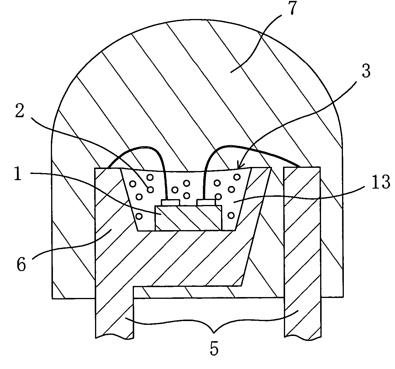
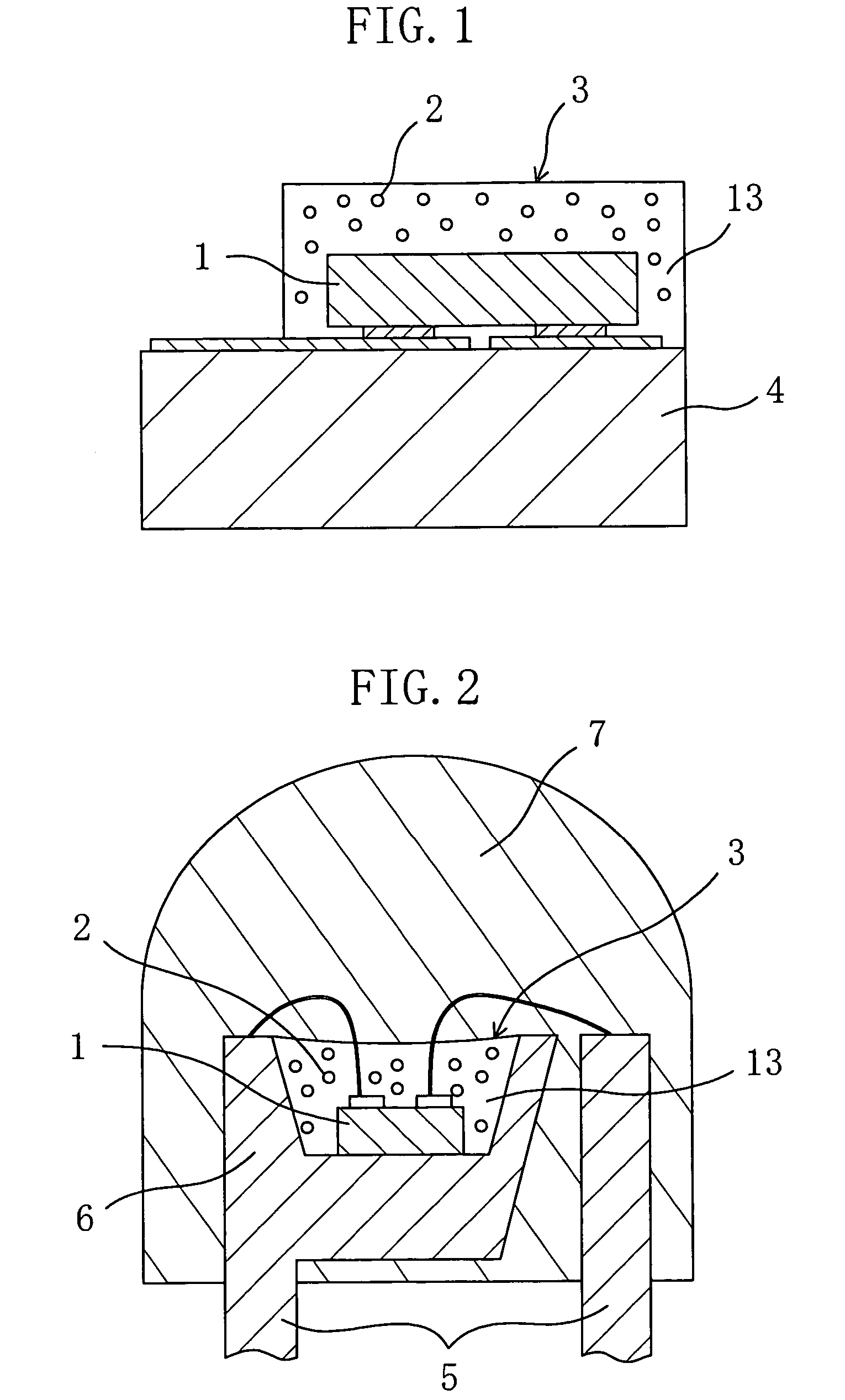
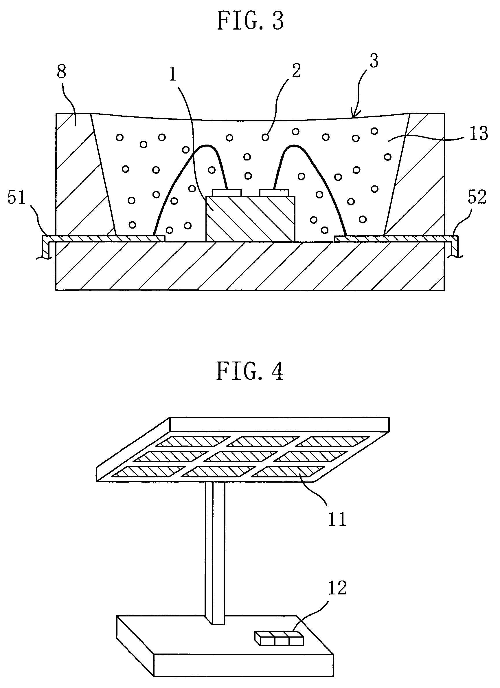
[0166]FIG. 1 is a vertical cross-sectional view showing a first exemplary light-emitting semiconductor device as a relatively typical example of this embodiment. As shown in FIG. 1, the first exemplary light-emitting semiconductor device is a chip-type light-emitting semiconductor device including: a substrate 4 (a submount element) functioning as a Zener diode; a flip-chip-type blue LED 1 mounted on the substrate 4 to be electrically connected to the Zener diode in the substrate; and a luminescent layer 3 encapsulating the blue LED 1 and made of a mixture of yellow / yellowish phosphor particles 2 and a base material 13 (a translucent resin). The blue LED 1 has a main light-extracting surface facing upward as shown in FIG. 1. The lumines...

embodiment 2

[0240]Now, an embodiment of a light-emitting system according to the present invention is described with reference to the drawings.

[0241]Various kinds of displaying systems using light-emitting semiconductor devices (e.g., LED information display terminals, LED traffic lights, LED stoplights of vehicles and LED directional lights) and various kinds of lighting systems (e.g., LED interior / exterior lights, courtesy LED lights, LED emergency lights, and LED surface emitting sources) are herein defined broadly as light-emitting systems.

[0242]FIGS. 4 through 6 are perspective views respectively showing examples of a light-emitting system according to a second embodiment of the present invention. FIG. 4 is a perspective view schematically showing a configuration of a desk-lamp-type lighting system as a first exemplary light-emitting system of the present invention.

[0243]As shown in FIG. 4, the first exemplary light-emitting system includes: a lighting unit in which a large number of light...

embodiment 3

[0428]In this embodiment, a method for forming a thin luminescent layer is described. According to this embodiment, yellow / yellowish phosphor particles which are expressed by the chemical formula (Sr1−a1−b1−xBaa1Cab1Eux)2SiO4 where the values a1, b1 and x are in the ranges 0≦a1≦0.3, 0≦b1≦0.8 (more preferably 0≦b1≦0.6) and 0

[0429]Hereinafter, examples of the fabrication method will be descr...


PUM


Abstract

A chip-type light-emitting semiconductor device includes: a substrate 4; a blue LED 1 mounted on the substrate 4; and a luminescent layer 3 made of a mixture of yellow / yellowish phosphor particles 2 and a base material 13 (translucent resin). The yellow / yellowish phosphor particles 2 is a silicate phosphor which absorbs blue light emitted by the blue LED 1 to emit a fluorescence having a main emission peak in the wavelength range from 550 nm to 600 nm, inclusive, and which contains, as a main component, a compound expressed by the chemical formula: (Sr1−a1−b1−xBaa1Cab1Eux)2SiO4 (0≦a1≦0.3, 0≦b1≦0.8 and 0<x<1). The silicate phosphor particles disperse substantially evenly in the resin easily. As a result, excellent white light is obtained.

Description

TECHNICAL FIELD[0001]The present invention relates to light-emitting semiconductor devices utilizing blue-light-emitting diodes (hereinafter, referred to as blue LEDs) and yellow / yellowish phosphors in combination to emit white light, light-emitting systems using the light-emitting semiconductor devices, and methods for fabricating the light-emitting semiconductor devices.BACKGROUND ART[0002]A light-emitting semiconductor device utilizing a blue LED (strictly speaking, a blue LED chip) having a main emission peak in the blue wavelength range from 400 nm to 530 nm, both inclusive, and a luminescent layer containing an inorganic phosphor (hereinafter, simply referred to as a “phosphor”) that absorbs blue light emitted by the blue LED and produces a fluorescence having an emission peak within a visible wavelength range from green to yellow (in the range of about 530 nm to about 580 nm) in combination is known to date. Light emitted from an LED that excites a phosphor is herein referred...

Claims


Application Information

Patent Timeline
Patent Type & Authority Patents(United States)
IPC IPC(8): H01L33/00H01L33/32H01L33/50H01L33/56H01L33/60H01L33/62
CPCC09K11/025C09K11/7734C09K11/7735C09K11/7774C09K11/7792F21S6/003H01L33/502H05B33/14C09K11/7731H01L24/45F21S6/00F21Y2101/02H01L33/54Y02B20/181H01L2924/12041H01L2224/8592H01L2224/48257H01L2224/73265H01L2224/48247H01L2224/48227H01L2224/48091H01L2224/32225H01L2224/16145H01L2224/45144H01L2224/45124H01L2924/00014H01L2924/00H01L2924/12035H01L2924/12042H01L2924/12044H01L2924/181F21Y2115/10Y02B20/00C09K11/77342H01L2924/00012
Inventor MAEDA, TOSHIHIDEOSHIO, SHOZOIWAMA, KATSUAKIKITAHARA, HIROMIIKEDA, TADAAKIKAMEI, HIDENORIHANADA, YASUYUKISAKANOUE, KEI
Owner PANASONIC CORP
Why Eureka
Try Eureka