Variable gain amplifier

Inactive Publication Date: 2006-04-04
SHARP KK
View PDF10 Cites 25 Cited by
  • Summary
  • Abstract
  • Description
  • Claims
  • Application Information

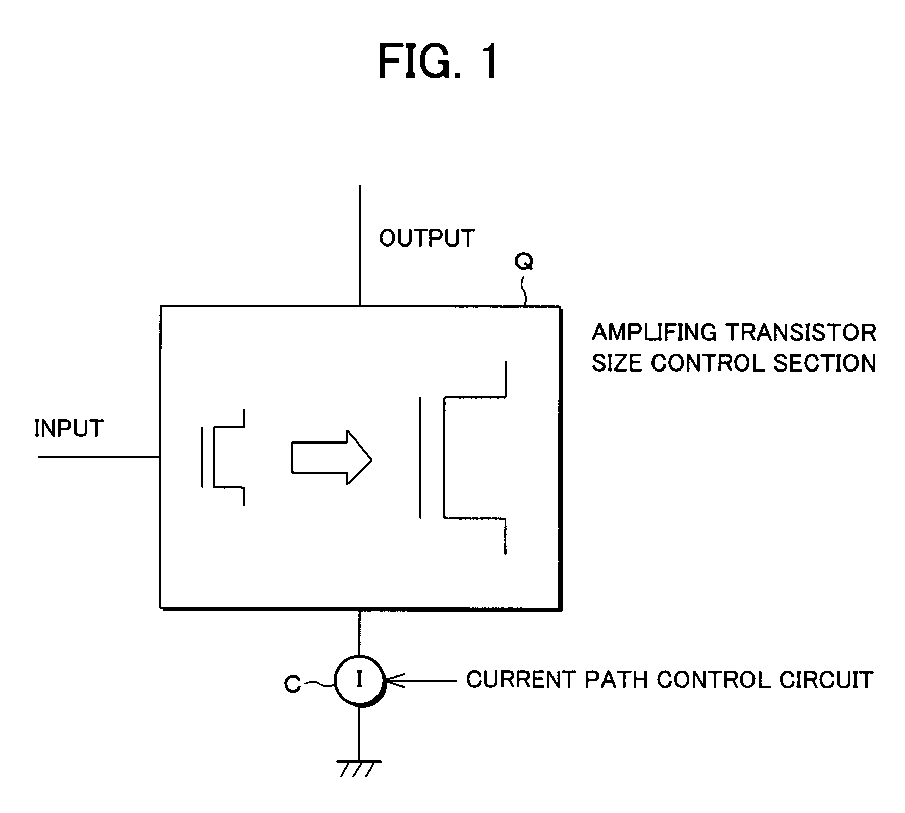
AI Technical Summary

Benefits of technology

[0011]It is an object of the present invention to provide variable gain amplifiers with a small

Problems solved by technology

However, the PIN diodes cannot be formed on a common semiconductor integrated circuit such as a CMOS or bipolar semiconductor integrated circuit.
Firstly, accurate designing of the resistor ladder requires a low ON resistance for the nMOS transistors switches Mn1, Mn2, Mn3, . However, in order to fabricate a switch with an ON resistance of 1 Ω using, for example, a standard CMOS process of 0.25 μm, a gigantic transistor with a channel width of 1000 μm will be required. The resistor ladder requires a plurality of such gigantic transistors. The result of this is an increased mount area.
Secondly, a change in resistance value of the variable resistor 1Re varies the value of the current in the circuit, which causes the operating point of the transistors to fluctuate. This fluctuation of the operating point is suppressed by the provision of an adjuster circuit of a bias voltage Vb, as

Method used


Image

  • Variable gain amplifier
  • Variable gain amplifier
  • Variable gain amplifier

Examples


first embodiment

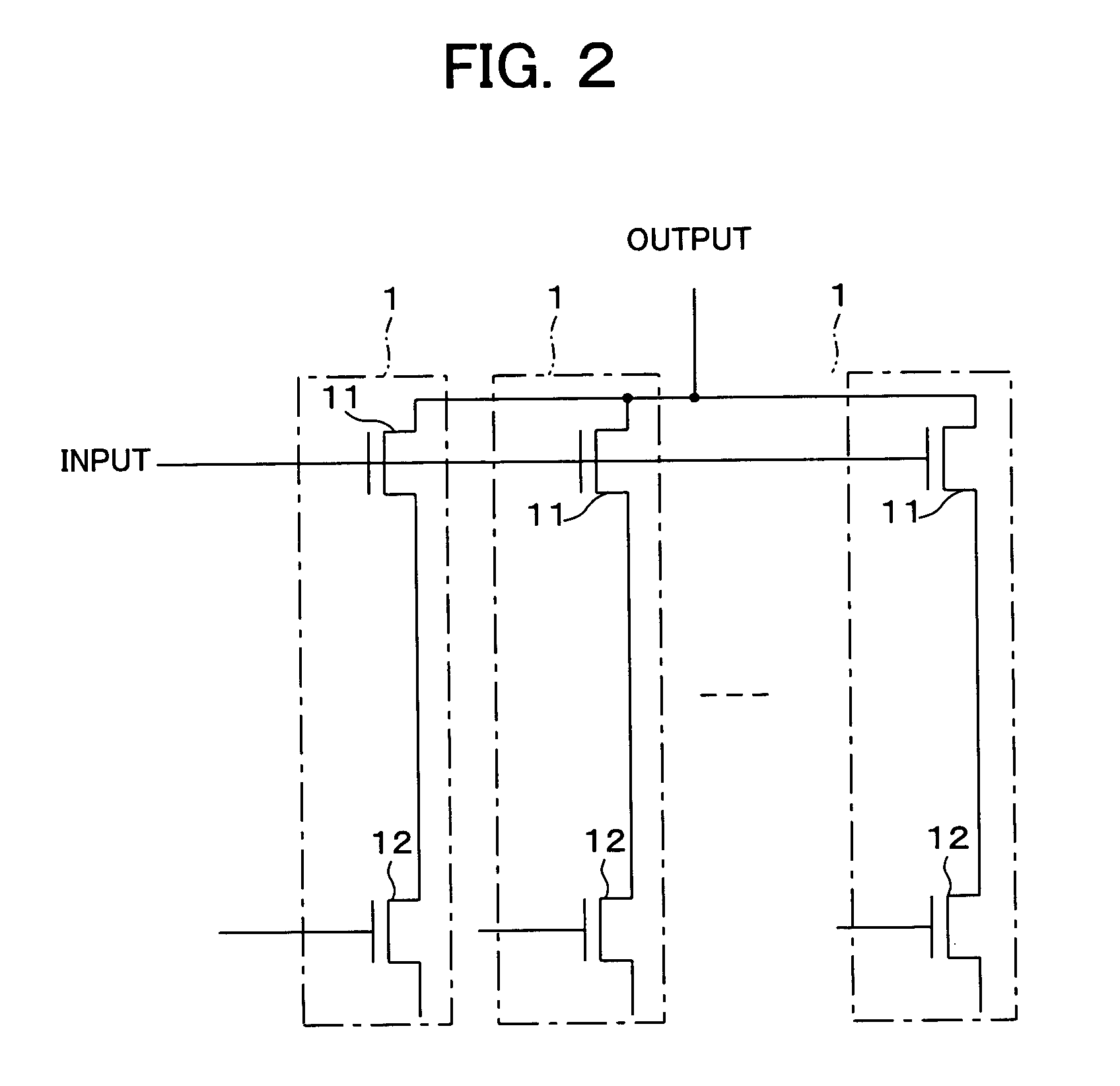
[0052][First Embodiment]

[0053]A variable gain amplifier according to this embodiment, as shown in FIG. 2, includes a plurality of unit circuits 1, each having a signal input transistor 11 (amplifying transistor) and a current control transistor 12. In the unit circuit 1, the source of the signal input transistor 11 is connected to the drain of the current control transistor 12, and the signal from the drain of the signal input transistor 11 becomes the output of the circuit. The plurality of unit circuits 1 are disposed in parallel, and are connected to one another through the inputs (gate of the signal input transistor 11) and outputs of a signal, so as to make up a variable transconductance (voltage current gain) circuit with a plurality of control inputs.

[0054]In the variable transconductance circuit having such a configuration, the current through each unit circuit 1 (signal input transistor 11) can be independently controlled by controlling the gate voltage of the current contr...

second embodiment

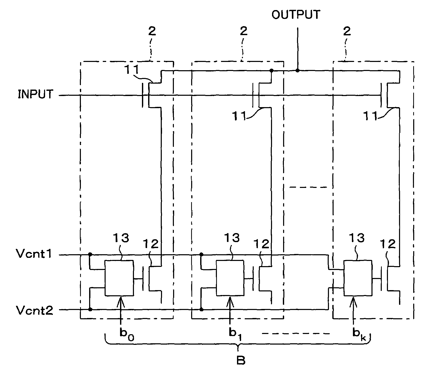
[0056][Second Embodiment]

[0057]A variable gain amplifier according to this embodiment, as shown in FIG. 3(a), includes a plurality of unit circuits 2, each having a current control switch 13 in addition to the structure of the unit circuit 1 of the variable gain amplifier of FIG. 2. The current control switch 13 (switch control circuit) is operable to select a current control voltage Vcnt1 or Vcnt2 in accordance with a switch control signal B, so as to feed it as a gate voltage (operation control voltage) to the gate (input section) of the current control transistor 12. The switch control signal B is a digital signal of multiple bits b0, b1, . . . , bk (where k is an integer of not less than 0) which are respectively inputted to the unit circuits 2.

[0058]Under normal operating conditions, the switch control signal B is generated in accordance with the input signal or output signal, so that the signal level of the output becomes constant.

[0059]Note that, the configuration shown in FI...

third embodiment

[0070][Third Embodiment]

[0071]As shown in FIG. 8, a variable gain amplifier according to this embodiment is configured to realize the functions of the variable gain amplifiers of the FIG. 4 through FIG. 7 with a simple structure, using a MOS transistor. Specifically, the variable gain amplifier includes, instead of the unit circuits 2, a plurality of unit circuits 3, each having a current control transistor 14 (auxiliary current control transistor) and a current source 15, in addition to the configuration of the unit circuit 2.

[0072]The unit circuits 3, as with the unit circuits 2, are disposed in parallel, and are connected to one another through the signal inputs and signal outputs.

[0073]The source of the signal input transistor 11 is connected to the drain of the current control transistor 12, and the gate of the current control transistor 12 is connected to the gate of the current control transistor 14 and to the output terminal of the current control switch 13. One input termin...


PUM


Abstract

A variable gain amplifier includes a current path control circuit which controls a path of a current flow through an amplifying transistor section, so as to control the actual size of transistors which make up the amplifying transistor section, and thereby control the gain and IIP3 (third-order Input Intercept Point). When the size W/L of the transistors is decreased or increased under constant current level maintained in a current path control circuit in the circuit, the transconductance (gain) is decreased or increased and the IIP3 is increased or decreased. According to this principle, there is provided a variable gain amplifier with a small mount area, capable of compensating for a decrease of the gain by an increase of the IIP3.

Description

FIELD OF THE INVENTION[0001]The present invention relates to highly linear variable gain amplifiers having semi conductor element components, and particularly to variable gain amplifiers which are effective in realizing broadband wireless communication devices.BACKGROUND OF THE INVENTION[0002]Broadband wireless communication devices such as a tuner used in television broadcasts via cable transmission or wireless transmission require a variable gain amplifier with high linearity (small distortion) to suppress intermodulation interference between different channels in response to input of a strong signal. Conventional tuners made up of discrete parts have adopted an attenuator with highly linear PIN diode components to prevent entry of a strong signal into the amplifier and thus suppress an intermodulation interference signal. However, the PIN diodes cannot be formed on a common semiconductor integrated circuit such as a CMOS or bipolar semiconductor integrated circuit. Thus, in order...

Claims


Application Information

Patent Timeline
IPC IPC(8): H03F3/45H03G3/10H03G3/30
CPCH03G3/3042H03F3/45183
Inventor MIYAMOTO, MASAYUKI
Owner SHARP KK
Why Eureka
Try Eureka