Method of improving copper pad adhesion

a technology of copper pads and metal structures, applied in the direction of semiconductor devices, semiconductor/solid-state device details, electrical apparatus, etc., to achieve the effect of increasing the area occupied by metal lines, reducing contact resistance, and increasing device speed

Inactive Publication Date: 2006-04-11
TAIWAN SEMICON MFG CO LTD
View PDF61 Cites 24 Cited by
  • Summary
  • Abstract
  • Description
  • Claims
  • Application Information

AI Technical Summary

Benefits of technology

[0013]U.S. Pat. No. 5,795,796 (Kim) shows an Al interconnect with a TaN barrier layer. A method of fabricating a metal line includes the steps of preparing a semiconductor substrate, depositing a first metal on the semiconductor substrate, heat-treating the first metal to form a first metal nitride layer. depositing a second metal on the first metal nitride layer. heat treating the second metal. depositing a third metal on the second metal, and heat treating both the third metal and the second metal to form a metal insulating layer in which the second and the third metals are mixed. The method of fabricating increases the area occupied by the metal line in a contact hole, decreases contact resistance, and increases the speed of the device.
[0014]U.S. Pat. No. 5,668,411 (Hong at al.) shows a Al / TaN / Al structure with an anneal step. A diffusion barrier trilayer is comprised of a bottom layer, a seed layer and a top layer. The diffusion barrier trilayer prevents reaction of metallization layer with the top layer upon heat treatment, resulting in improved sheet resistance and device speed.

Problems solved by technology

However, using this method is only a partial solution to a wire bonding adhesion problem.

Method used


Image

  • Method of improving copper pad adhesion
  • Method of improving copper pad adhesion
  • Method of improving copper pad adhesion

Examples


Embodiment Construction

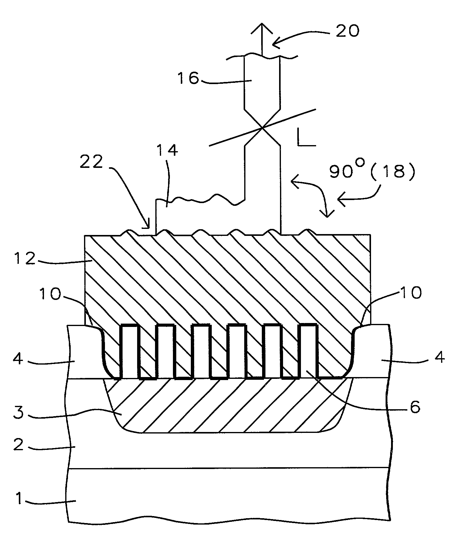
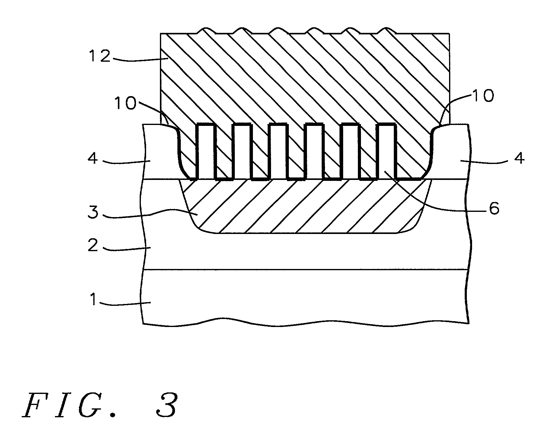
[0035]The present invention is a new and improved method for fabricating aluminum metal pad structures. A “standard” damascene process is used with copper interconnect metallization and large copper pad contacts to tungsten plugs (not shown in Figures). For better adhesion, the “convention” solution is the addition of tantalum nitride, TaN, as a barrier layer and the deposition of an AlCu pad on the surface. However, using this method is only a partial solution to the wire bonding problem. This invention describes a new method for improved wire bond pad adhesion in which a special via hole interlocking structure is fabricated between the TaN barrier layer and Al pad structure.

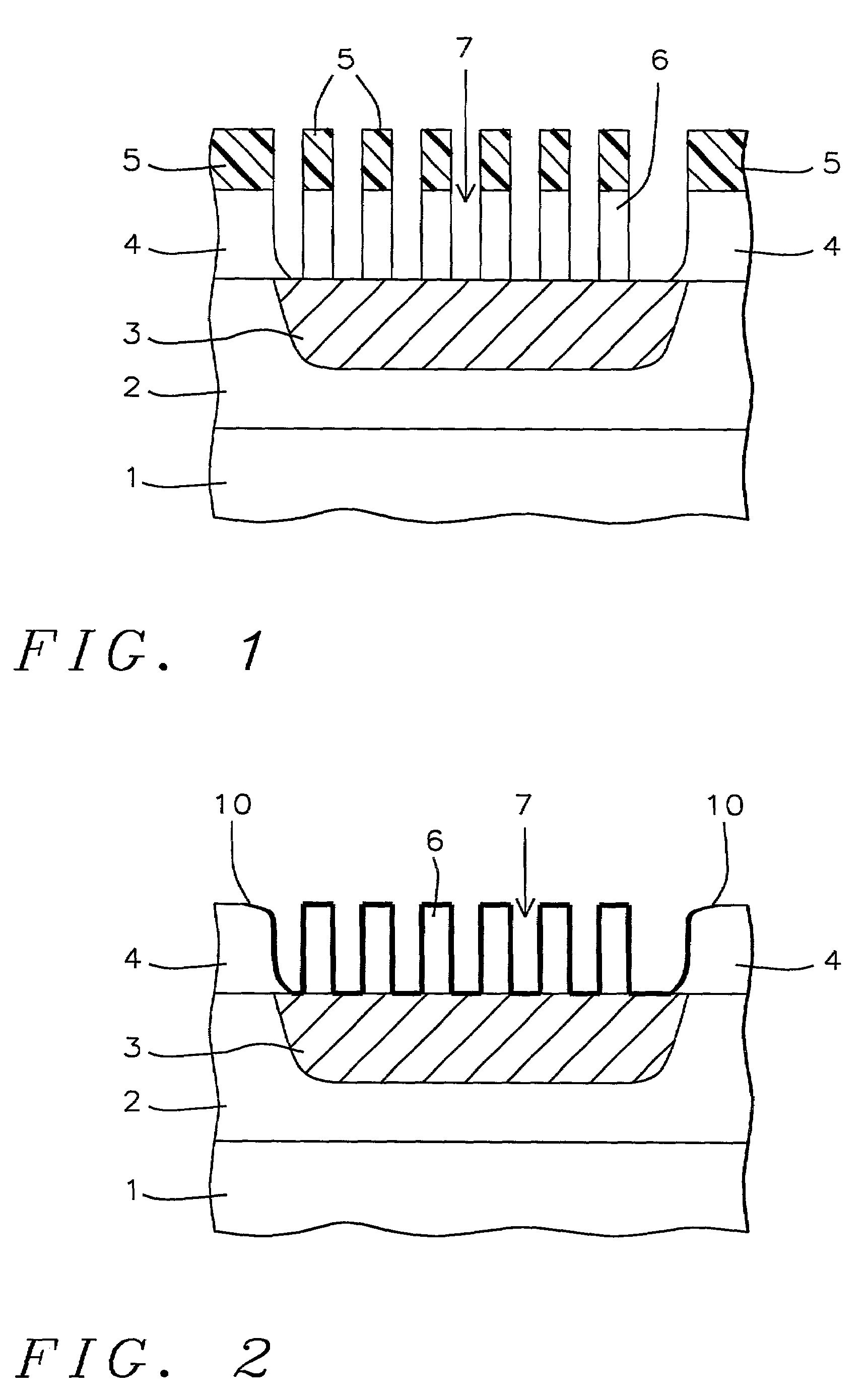
[0036]Referring to FIG. 1, which in cross-sectional representation, shows a semiconductor silicon substrate 1 (or an IC module) with the first level of metal copper wiring 3 being defined, embedded in the first layer of insulator 2, typically silicon oxide SiOX. The invention starts with these conventional laye...


PUM

PropertyMeasurementUnit
heightaaaaaaaaaa
widthaaaaaaaaaa
widthaaaaaaaaaa

Abstract

This invention relates to a new improved method and structure in the fabricating of aluminum metal pads. The formation special aluminum bond pad metal structures are described which improve adhesion between the tantalum nitride pad barrier layer and the underlying copper pad metallurgy by a special interlocking bond pad structure. It is the object of the present invention to provide a process wherein a special grid of interlocking via structures is placed in between the underlying copper pad metal and the top tantalum nitride pad barrier layer providing improved adhesion to the aluminum pad metal stack structure. This unique contact bond pad structure provides for thermal stress relief, improved wire bond adhesion to the aluminum pad, and prevents peeling during wire bond adhesion tests.

Description

[0001]This is a division of patent application Ser. No. 09 / 442,497, filing date Nov. 18, 1999 now U.S. Pat. No. 6,191,023, Method Of Improving Copper Pad Adhesion, assigned to the same assignee as the present invention.BACKGROUND OF THE INVENTION[0002](1) Field of the Invention[0003]This invention relates to a method of fabrication used for semiconductor integrated circuit devices, and more specifically to the formation of aluminum pad metal structures are described which improve adhesion between the tantalum nitride pad barrier layer and the underlying copper pad metallurgy by a special interlocking via structure. It is the object of the present invention to provide a process wherein a special grid of interlocking via structures is placed in between the underlying copper pad metal and the top tantalum nitride pad barrier layer providing improved adhesion to the aluminum pad metal stack structure. This unique contact pad structure provides for thermal stress relief, improved wire bo...

Claims


Application Information

Patent Timeline
Patent Type & Authority Patents(United States)
IPC IPC(8): H01L31/00H01L21/44H01L23/52H01L21/60H01L23/485
CPCH01L24/03H01L24/05H01L24/11H01L24/48H01L2224/45124H01L2224/45144H01L2224/4807H01L2224/48458H01L2224/4847H01L2224/48624H01L2224/859H01L2924/01005H01L2924/01006H01L2924/01007H01L2924/01012H01L2924/01013H01L2924/01014H01L2924/01015H01L2924/01029H01L2924/01073H01L2924/01074H01L2924/01079H01L2924/014H01L2924/04953H01L2924/05042H01L2924/13091H01L2924/14H01L2924/19041H01L2924/20753H01L24/45H01L2224/04042H01L2224/05073H01L2224/05187H01L2224/05558H01L2224/05624H01L2224/13099H01L2224/45015H01L2924/01024H01L2924/01033H01L2224/05557H01L2224/05559H01L2224/45147H01L2224/48724H01L2224/48799H01L2924/10253H01L2224/0401H01L2924/00014H01L2924/04941H01L2924/00H01L2224/48824H01L2924/00011H01L2924/351H01L2924/00015
Inventor CHEN, SHENG-HSIUNG
Owner TAIWAN SEMICON MFG CO LTD
Why Eureka
Try Eureka