Integrated circuit substrate having laser-exposed terminals

Inactive Publication Date: 2006-04-18
AMKOR TECH SINGAPORE HLDG PTE LTD
View PDF36 Cites 55 Cited by
  • Summary
  • Abstract
  • Description
  • Claims
  • Application Information

AI Technical Summary

Benefits of technology

[0008]The above objectives of providing improved interconnect density and a low associated manufacturing cost and providing improvements in selectively plating terminals without a masking or resist process are provided in a

Problems solved by technology

The above-incorporated patent application “INTEGRATED CIRCUIT SUBSTRATE HAVING LASER-EMBEDDED CONDUCTIVE PATTERNS AND METHOD THEREFOR” provides increased conductor density and decreased inter-conductor spacing via laser-embedded circuit technolo

Method used


Image

  • Integrated circuit substrate having laser-exposed terminals
  • Integrated circuit substrate having laser-exposed terminals
  • Integrated circuit substrate having laser-exposed terminals

Examples


Example

[0015]The invention, as well as a preferred mode of use and advantages thereof, will best be understood by reference to the following detailed description of illustrative embodiments when read in conjunction with the accompanying drawings, wherein like reference numerals indicate like parts throughout.

DETAILED DESCRIPTION

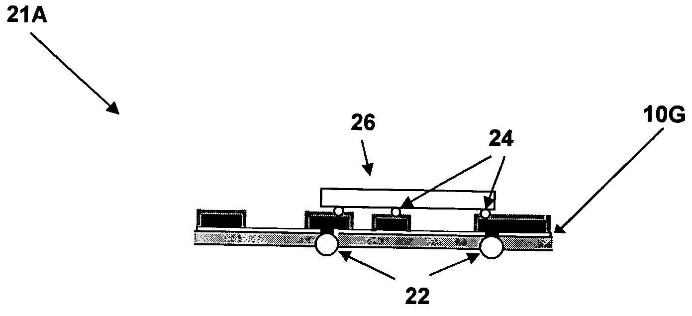
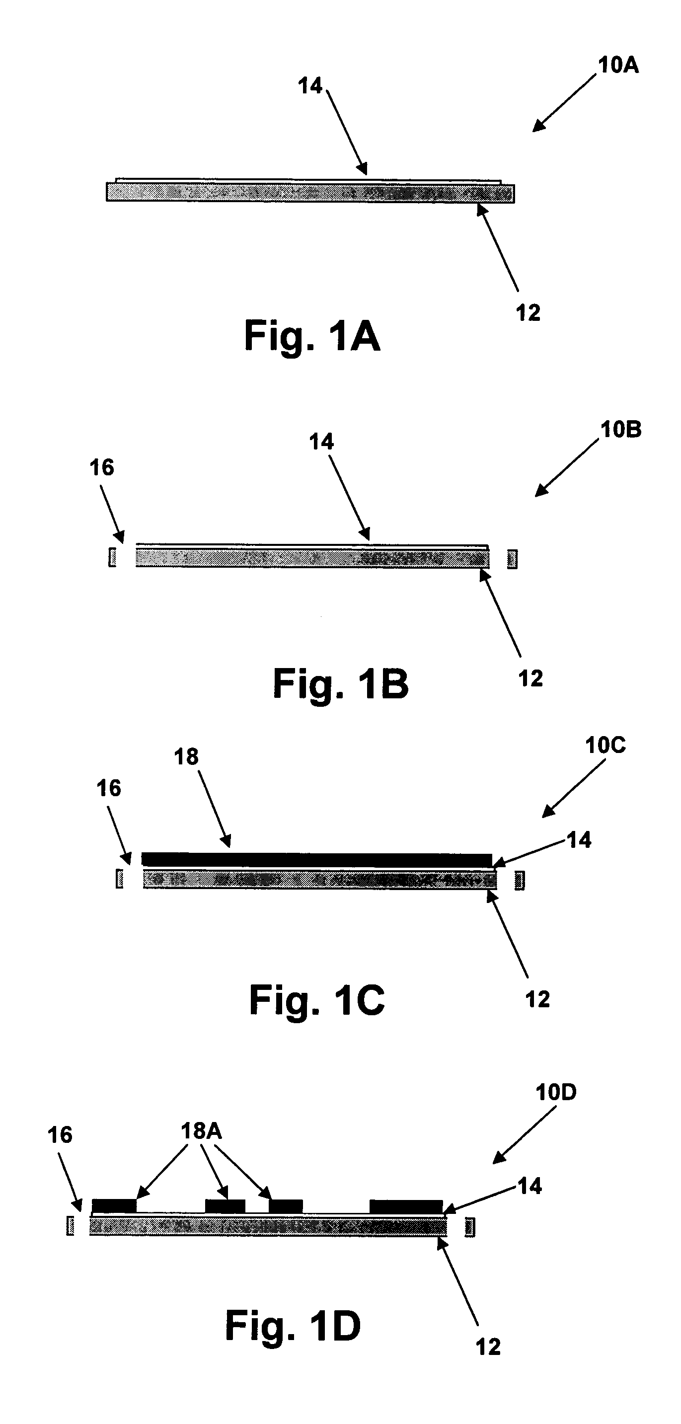
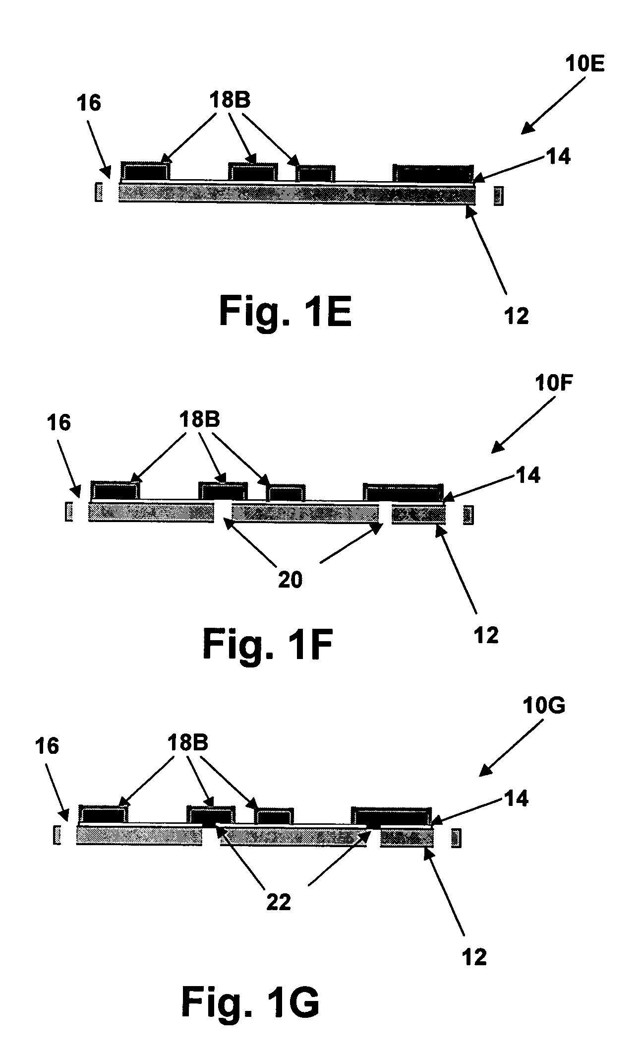
[0016]Referring now to the figures and in particular to FIGS. 1A through 1G, a cross-sectional view of stages of preparation of a substrate in accordance with an embodiment of the present invention is shown. A first substrate stage 10A, having a dielectric layer 12 and an adhesive layer 14 disposed thereon is punched to add sprocket holes 16 forming substrate stage 10B of FIG. 1B. Sprocket holes 16 are added for machine feeding the substrate stages, which are generally formed on a continuous tape, through processing machines for performing the method that prepares the substrate of the present embodiment. Substrate stage 10A may be fabricated from a dielectric film t...


PUM

PropertyMeasurementUnit
Dielectric polarization enthalpyaaaaaaaaaa
Densityaaaaaaaaaa
Electrical conductoraaaaaaaaaa

Abstract

An integrated circuit substrate having laser-exposed terminals provides a high-density and low cost mounting and interconnect structure for integrated circuits. The laser-exposed terminals can further provide a selective plating feature by using a dielectric layer of the substrate to prevent plating terminal conductors and subsequently exposing the terminals via laser ablation. A metal layer may be coated on one or both sides with a dielectric material, conductive material embedded within the dielectric to form conductive interconnects and then coating over the conductive material with a conformal protective coating. The protectant is then laser-ablated to expose the terminals. A dielectric film having a metal layer laminated on one side may be etched and plated. Terminals are then laser-exposed from the back side of the metal layer exposing unplated terminals.

Description

CROSS-REFERENCE TO RELATED APPLICATIONS[0001]The present application is a continuation-in-part of U.S. patent application entitled “INTEGRATED CIRCUIT SUBSTRATE HAVING LASER-EMBEDDED CONDUCTIVE PATTERNS AND METHOD THEREFOR”, Ser. No. 10 / 138,225 filed May 1, 2002, now U.S. Pat. No. 6,930,256, having at least one common inventor and assigned to the same assignee.[0002]The present application is also a continuation-in-part of U.S. patent application entitled “INTEGRATED CIRCUIT SUBSTRATE HAVING EMBEDDED BACK-SIDE ACCESS CONDUCTORS AND VIAS”, Ser. No. 10 / 392,737 filed Mar. 19, 2003, now abandoned, by the same inventors and assigned to the same assignee. The specifications of the above-referenced patent applications are herein incorporated by reference.FIELD OF THE INVENTION[0003]The present invention relates generally to semiconductor packaging, and more specifically, to a substrate having laser ablated terminals for conductors for providing an electrical interface between a die and ext...

Claims


Application Information

Patent Timeline
IPC IPC(8): H01K3/10
CPCH05K3/243H05K3/28H05K3/4007H05K1/056Y10T29/49165H05K3/107H05K3/244H05K3/386H05K2201/0394H05K2201/09472H05K2203/041H05K2203/072Y10T29/4913Y10T29/49117Y10T29/49144H05K3/0035
Inventor HINER, DAVID JONHUEMOELLER, RONALD PATRICKRUSLI, SUKIANTO
Owner AMKOR TECH SINGAPORE HLDG PTE LTD
Why Eureka
Try Eureka