
Semiconductor photocathode and photoelectric tube using the same

Inactive Publication Date: 2006-04-18
HAMAMATSU PHOTONICS KK
View PDF7 Cites 10 Cited by
  • Summary
  • Abstract
  • Description
  • Claims
  • Application Information

AI Technical Summary

Benefits of technology

[0010]Therefore, it is necessary to use a semiconductor material as the light absorbing layer in order to detect longer wavelength light within an infrared region. Further, it would be advantageous if the semiconductor material were able to be grown epitaxially, be direct transition type, have large absorption coefficient, and have a smaller energy band gap.
[0018]That is, in order to prevent recombination of electrons and holes which is caused by the connection of the valence band of GaSb and the valence band of InAsSb in GaSb substrate and InAsSb light absorbing layer, the first compound semiconductor layer (hole blocking layer having a wide band gap) is inserted between the substrate and the light absorbing layer, so that the valence band of the GaSb substrate and the conduction band of the InAsSb light absorbing layer are separated to each other. As the result, the hole blocking layer (the first compound semiconductor layer) prevents electrons generated in the light absorbing layer from recombining holes from the substrate so that they annihilate. Therefore, the cut-off wavelength within the sensitive wavelength is increased.
[0020]As a result of this structure, it also becomes possible to block the flow of holes from the contact layer to the light absorbing layer, the contact layer being formed on the opposite side of the semiconductor substrate from the light absorbing layer, therefore, the electrons exit the photocathode efficiently.
[0024]Further, when the AlSb / GaSb superlattice structure is used as the first compound semiconductor layer that is positioned between the semiconductor substrate and the light absorbing layer, it can function as a superlattice buffer layer between the semiconductor substrate and the light absorbing layer. As a result, the crystal defect can be reduced, and improved characteristics such as increased sensitivity and reduced a dark current realized.
[0027]When comprising the above semiconductor photocathode, the photomultiplier tube can detect a long wavelength side cut-off wavelength in a sensitive wavelength within an infrared region, with high sensitivity.

Problems solved by technology

However, light having longer wavelength within the infrared region cannot be detected because the photocathode described in the above publication can detect light having shorter infrared wavelengths.

Method used


Image

  • Semiconductor photocathode and photoelectric tube using the same
  • Semiconductor photocathode and photoelectric tube using the same
  • Semiconductor photocathode and photoelectric tube using the same

Examples


Embodiment Construction

[0037]The preferred embodiments of the present invention will be explained below on the basis of the drawings. Note that the same elements will be given the same reference numerals, and repetitive explanation will be omitted.

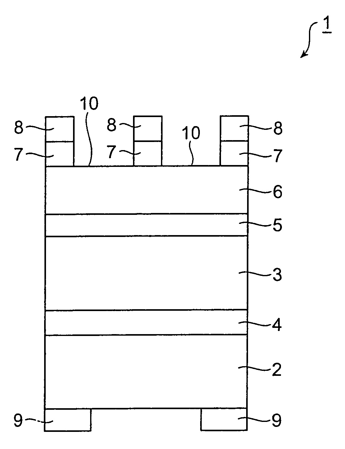
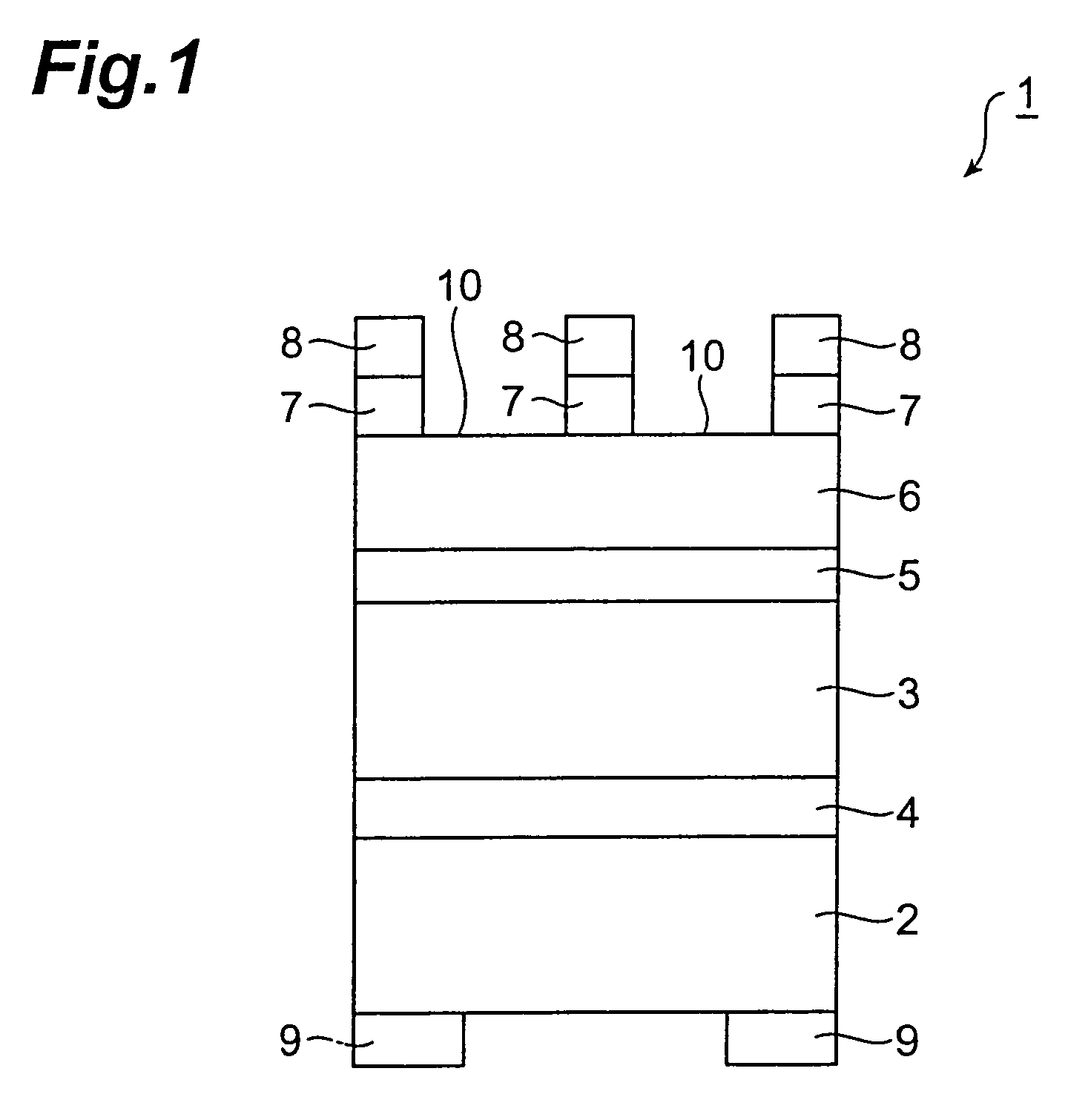
[0038]FIG. 1 is a diagram showing a semiconductor photocathode according to the first embodiment.

[0039]The semiconductor photocathode 1 shown in this figure comprises: a p+-type semiconductor substrate 2 made of GaSb; and a p−-type light absorbing layer 3 made of InAsSb.

[0040]A p+-type hole blocking layer 4 that is formed between semiconductor substrate 2 and light absorbing layer 3 has a wider energy band gap than that of light absorbing layer 3 and is made of AlGaSb.

[0041]Further, a p−-type hole blocking layer 5 of AlGaSb is formed on light absorbing layer 3, and a p−-type electron emitting layer 6 of GaSb is formed on hole blocking layer 5. An n+-type contact layer 7 of GaSb is formed on the electron emitting layer 6. This contact layer 7 and electron emittin...


PUM


Abstract

A semiconductor photocathode comprises a p+-type semiconductor substrate of GaSb, and a p−-type light absorbing layer of InAsSb. A p+-type hole blocking layer is formed between the substrate and the light absorbing layer having wider energy band gap than that of the light absorbing layer, the blocking layer being made of AlGaSb.

Description

BACKGROUND OF THE INVENTION[0001]1. Field of the Invention[0002]This invention relates to a semiconductor photocathode emitting photoelectrons in response the incidence of photons and a photoelectric tube using the same.[0003]2. Related Background Art[0004]In general, the detectable longer wavelength limit of a semiconductor photocathode is largely determined by the semiconductor energy band gap of the light absorbing layer. For example, the upper detectable limit of wavelength is about 1.7 μm in a crystal system that lattice matches to an InP substrate.[0005]On the other hand, a conventional photocathode is known that has a step-graded buffer layer on an InP substrate, wherein As to P composition ratio is gradually changed in the buffer layer (Japanese patent application laid-open No. 11-297191).[0006]In this photocathode, light within the infrared region extending to a wavelength of about 2.3 μm is detectable, because the lattice mismatch between the InP substrate and the InGaAs l...

Claims


Application Information

Patent Timeline
IPC IPC(8): H01L29/06H01L29/12H01J1/34H01J29/38H01J31/50H01J40/06H01J43/08
CPCH01J40/06H01J1/34
Inventor EDAMURA, TADATAKANIIGAKI, MINORU
Owner HAMAMATSU PHOTONICS KK
Learn More