Power semiconductor component in the planar technique

a semiconductor and planar technology, applied in semiconductor devices, basic electric elements, electric devices, etc., can solve the problems of inability to offer a solution, local increases in field strength, and reduction of maximum blocking voltage or parasitic blocking current, so as to achieve the effect of particularly effective increasing the maximum blocking voltag

Inactive Publication Date: 2006-04-18
IXYS SEMICON
View PDF20 Cites 33 Cited by
  • Summary
  • Abstract
  • Description
  • Claims
  • Application Information

AI Technical Summary

Benefits of technology

[0015]The invention is based on the knowledge that the parasitic blocking current, in the presence of an inversion layer (channel) produced by surface charges, essentially depends on the electrical resistance of this layer. The electrical surface resistance is increased with the surface structure according to the invention, as a result of which the effect of the surface charges is diminished and harmful field peaks are avoided.
[0017]The surface structure can in principle be differently constituted. In a preferred form of embodiment, the at least one depression of the surface structure is designed as an annular trench. It has been shown that the maximum blocking voltage can be particularly effectively increased when the ratio between the width and depth of the trenches is equal to or preferably less than 1. Trenches with a depth that is less than 15 μm and with a width that is smaller than their depth have proved to be particularly advantageous in practice.

Problems solved by technology

A further problem of the edge termination is the shielding of the chip edge against electric charges and chemical influences, which can cause local increases in field strength and a reduction in the maximum blocking voltage or parasitic blocking currents.
The guard rings can effectively reduce the surface field, but they do not offer any solution against the effect of surface charges, since the low-doped regions lying between the guard rings react very sensitively to freely mobile surface charges and polarisable molecules, and this can lead to an inversion of the surface and thus to a conductive connection between the guard rings.
When relatively high voltages are applied and a relatively deep inversion layer is formed, the channel stopper is unable to prevent the formation of a channel and parasitic leakage currents, if the inversion layer extends up to right next to the channel stopper and high field strengths are created there, which can lead to the injection of charge carriers into the space charge region.
But the junction termination extensions also have the same drawbacks as the guard rings.
The relatively costly production of the vertical edge termination is a drawback.
Moreover, the chip is weakened at the edge, which is a drawback especially during the handling and division of the wafer into individual chips.

Method used


Image

  • Power semiconductor component in the planar technique
  • Power semiconductor component in the planar technique
  • Power semiconductor component in the planar technique

Examples


Embodiment Construction

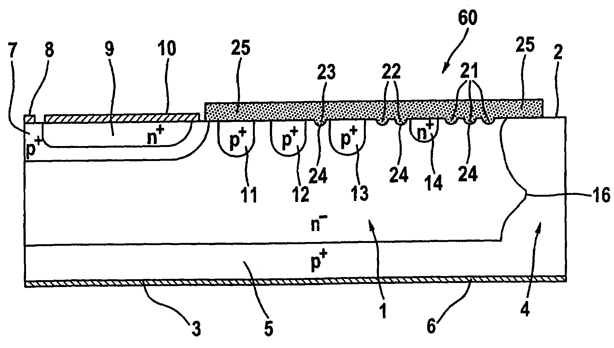
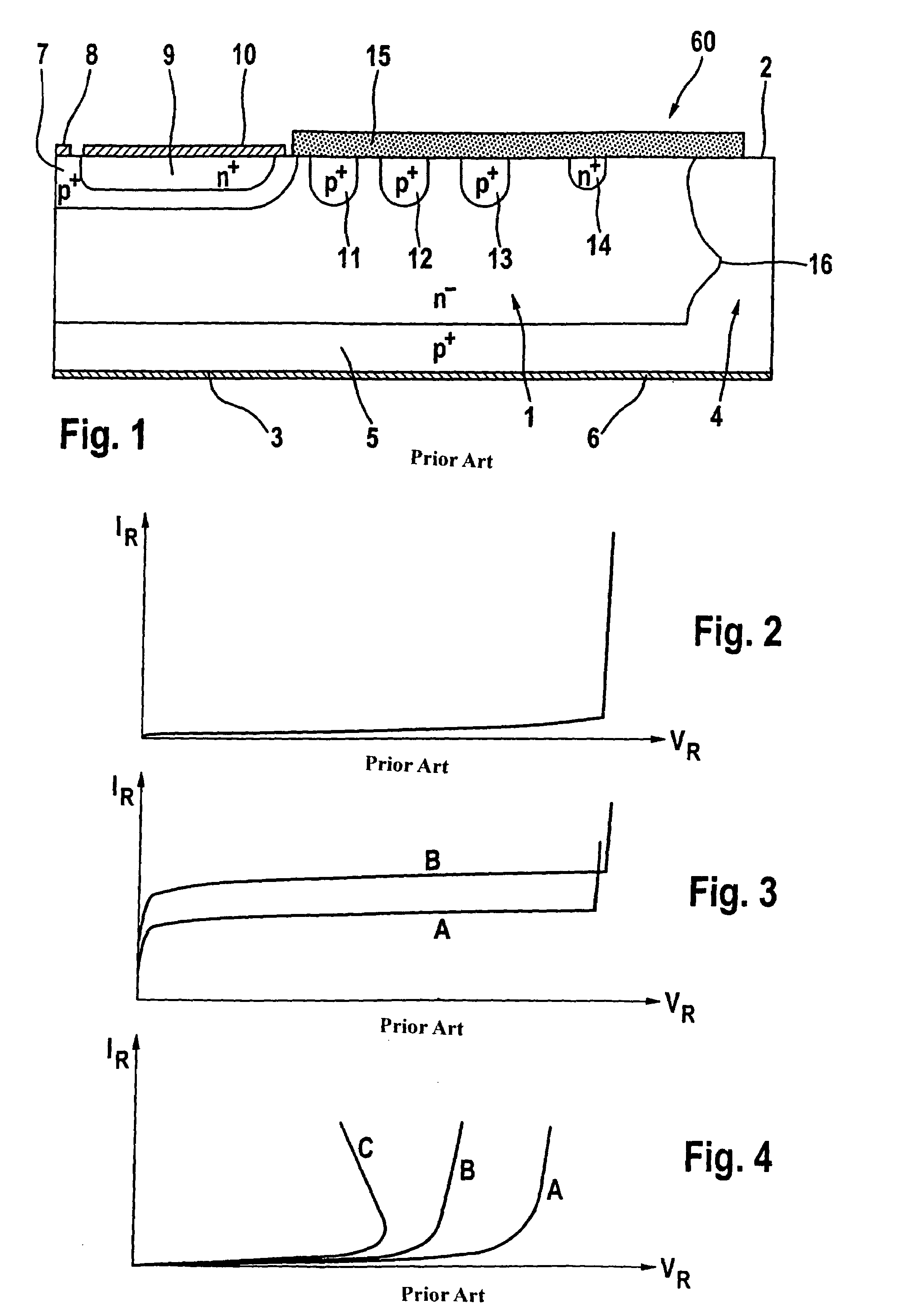
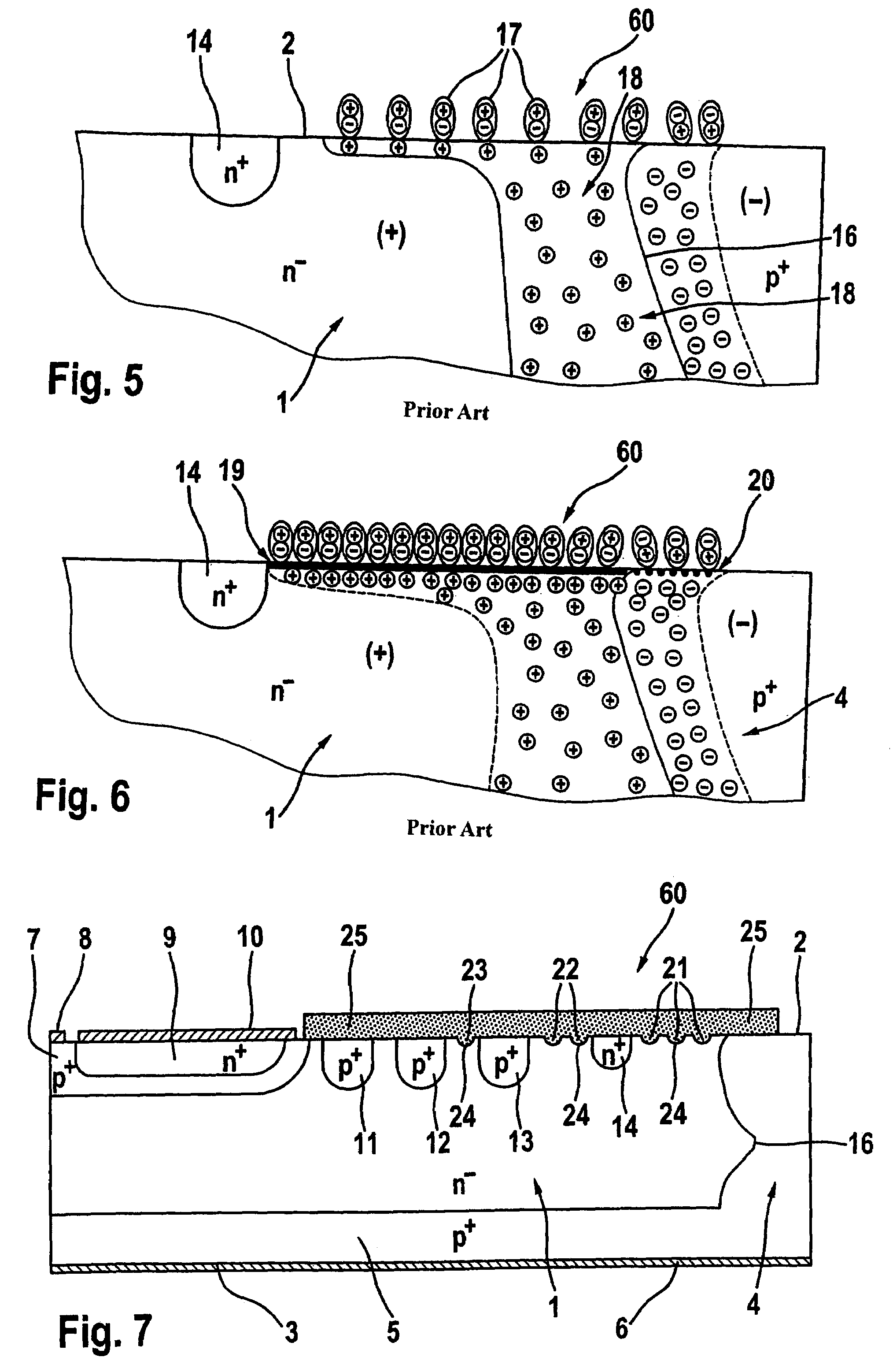
[0036]FIG. 1 shows a thyristor in cross-section produced according to the prior art in the planar technique. An n−-conductive silicon disc ((111)-Si), as semiconductor body 1, is used to produce the thyristor, said silicon disc having an upper main surface 2 and a lower main surface 3. The demarcation of the individual thyristors in the silicon disc 1 takes place with a p+-insulation diffusion from upper and lower main surface 2, 3, as a result of which a p+-conductive component edge 4 arises. With a further diffusion, a p+-conductive zone 5 is produced in the surface region adjacent to lower main surface 3. A pn-junction 16 arises, which extends in the edge region up to upper main surface 2. A full-surface anode metallic coating 6 is deposited on lower main surface 3.

[0037]A p+-conductive base layer 7 with a metallic coating 8 for the gate terminal is located in a first surface region adjacent to upper main surface 2. An n+-conductive zone 9 with a metallic coating 10 for the catho...


PUM


Abstract

In a power semiconductor component produced in a planar technique, a near-surface structure having at least one depression is formed in a surface region of an edge termination adjacent a main surface of the semiconductor body. The structure lies inside a space charge region formed when a voltage is applied at a junction between semiconductor regions of opposite conduction type. Dielectric material may fill the depression and form a passivation layer on the surface region. The depression may be an annular trench having a width to depth ratio ≦1. Alternatively, the structure may be waffle-shaped with multiple depressions.

Description

BACKGROUND OF THE INVENTION[0001]1. Technical Field[0002]The present invention relates to a power semiconductor component produced in the planar technique with a semiconductor body of the one conduction type, in whose surface region adjacent to a main surface there is embedded at least one semiconductor region of another conduction type opposite to the one conduction type.[0003]2. Background Information[0004]Power semiconductor components are characterised by a high electric strength. Examples of such semiconductor components are thyristors or diodes. In order to achieve a high maximum blocking voltage, the design of the edge termination of a semiconductor component is of particular importance. An essential problem of the edge termination lies in controlling the electric field strength in such a way that a premature breakdown is avoided in the case of blocking. In order to achieve this, the equipotential lines in the area of the chip edge have to be led in the case of blocking in a ...

Claims


Application Information

Patent Timeline
Patent Type & Authority Patents(United States)
IPC IPC(8): H01L29/68H01L29/06H01L29/78H01L31/0392
CPCH01L29/0661H01L29/7802H01L29/7811
Inventor NEIDIG, ARNO
Owner IXYS SEMICON
Why Eureka
Try Eureka