Tuneable electromagnetic bandgap structures based on high resistivity silicon substrates

Active Publication Date: 2006-04-18
UNIV OF DAYTON THE
View PDF13 Cites 38 Cited by
  • Summary
  • Abstract
  • Description
  • Claims
  • Application Information

AI Technical Summary

Benefits of technology

[0006]It is in view of the above mentioned background, that the present invention provides a number of unobvious advantages and advancements over the prior art. In particular, the above-mentioned problems are addressed by using high permittivity dielectrics (such as ceramics based on ferroelectrics) in an EBG structure according to the present invention. The present inventors have discovered that the use of low loss ferroel

Problems solved by technology

The main disadvantage of prior art EBG structures is their large size (e.g., greater than 3 centimeters) at low microwave frequencies, since the periodicity of the struct

Method used


Image

  • Tuneable electromagnetic bandgap structures based on high resistivity silicon substrates
  • Tuneable electromagnetic bandgap structures based on high resistivity silicon substrates
  • Tuneable electromagnetic bandgap structures based on high resistivity silicon substrates

Examples


Embodiment Construction

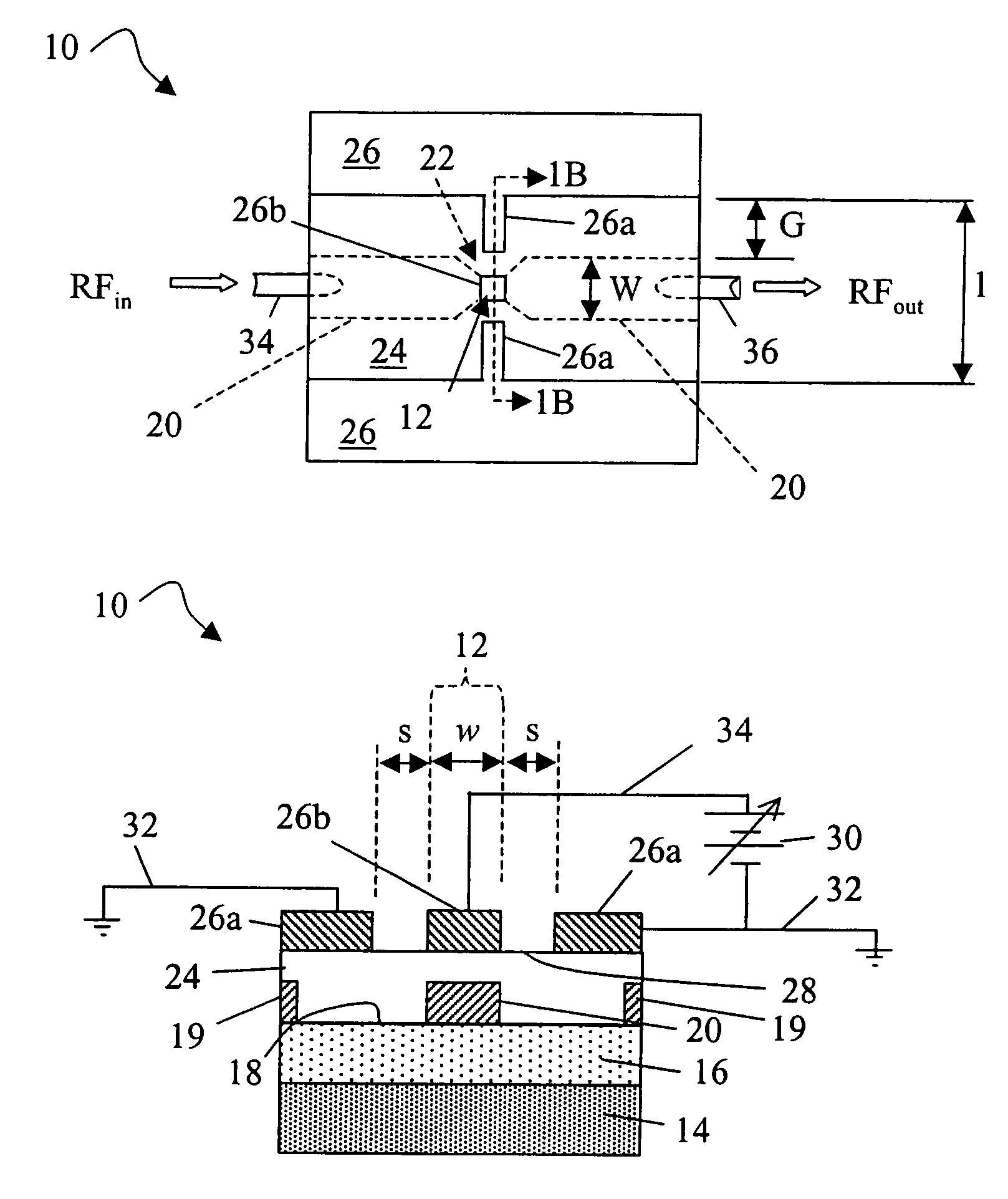
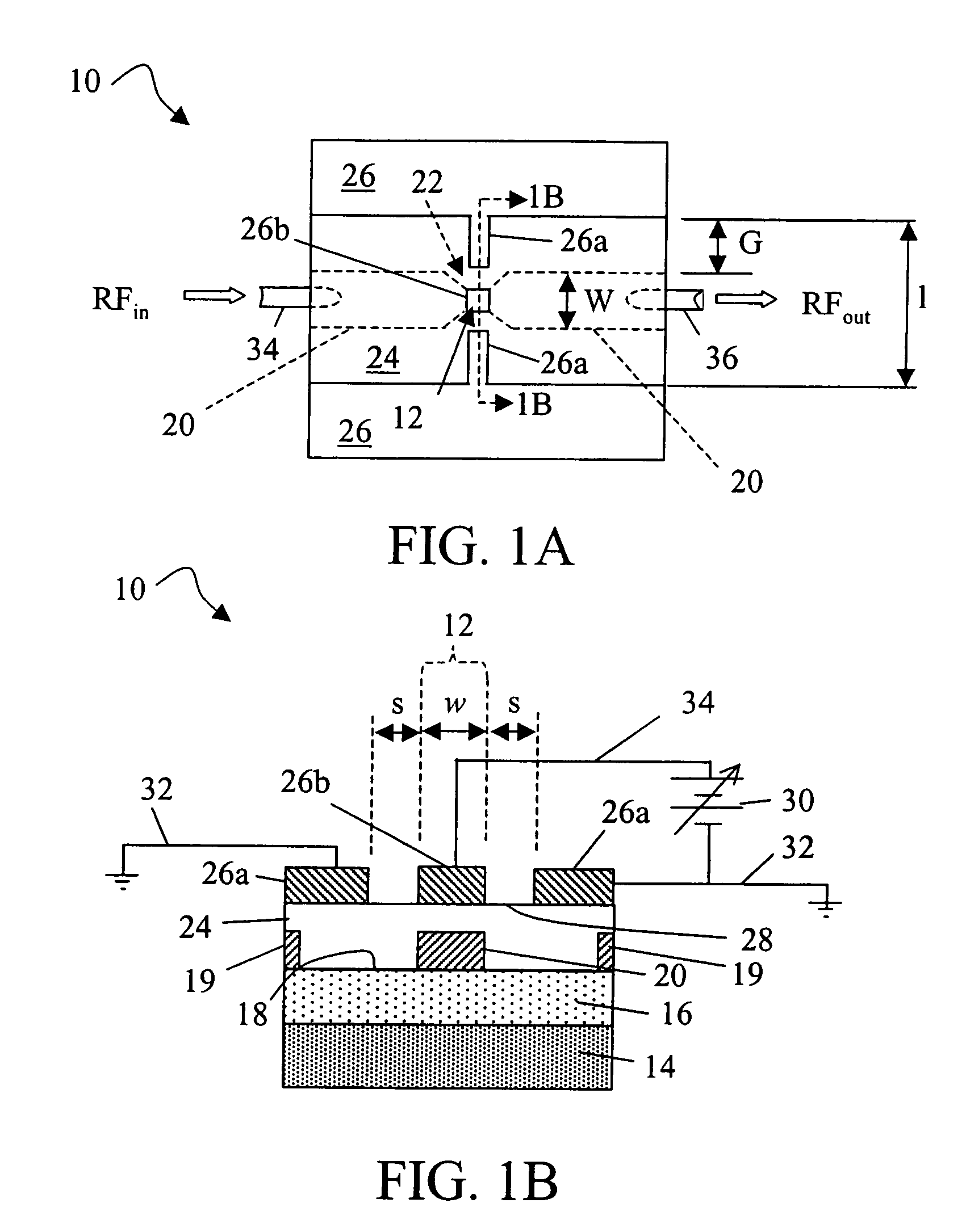
[0022]The present invention describes ferroelectric tunable electromagnetic band (“TEBG”) structures useful for periodically loading coplanar waveguides (“CPWs”). High dielectric permittivity of the ferroelectrics used in the present invention enables reduction of the wavelength in the line and hence the period of the TEBG structures. This helps to reduce the size of the TEBG structures according to the present invention by at least a factor of 2 or more, which pushes the application of TEBG structures to lower range of microwave frequencies, and facilitates the integration of TEBG structures into semiconductor substrates at millimeter / sub-millimeter waves.

[0023]Additionally, the TEBG structures according to the present invention may be operated in an environment having a temperature range of between about 77K to about 330K. Furthermore, the TEBG structures according to the present invention can handle up to 3 megavolts per centimeter, or in one embodiment, which provides a 40 μm ga...


PUM


Abstract

Electrically tunable electromagnetic bandgap (“TEBG”) structures using a ferroelectric thin film on a semiconductor substrate, tunable devices that include such a TEBG structure, such as a monolithic microwave integrated circuit (“MMIC”), and a method producing such a TEBG structure are disclosed. The present invention provides a semiconductive substrate having an oxide layer, a first conductive layer positioned on the oxide layer, a ferroelectric layer covering the first conductive layer, and a second conductive layer positioned on a surface of the tunable ferroelectric layer. The use of the ferroelectric layer, which have a DC electric field dependent permittivity, enables a small size, tunable EBG structure.

Description

CROSS REFERENCE TO RELATED APPLICATIONS[0001]This application claims the benefit of provisional application No. 60 / 507,785 filed on Oct. 1, 2003.BACKGROUND OF THE INVENTION[0002]The present invention relates generally to silicon-based structures and in particular, to a room-temperature, electrically tunable electromagnetic bandgap (“TEBG”) structure using a ferroelectric thin film on a semiconductor substrate, tunable devices that include such a TEBG structure, such as a monolithic microwave integrated circuit (“MMIC”), and a method producing such a TEBG structure.[0003]Prior art electromagnetic bandgap (“EBG”) structures are essentially one-, two-, and three-dimensional metal-dielectric and dielectric—dielectric periodic structures. EBG structures, known also as photonic bandgap (“PBG”) crystals, are extensively considered for applications in microwave devices, including filters, multiplexers, phase shifters, and frequency selective surfaces (“FSS”). In EBG structures, electromagne...

Claims


Application Information

Patent Timeline
IPC IPC(8): H01L29/93H01G5/00
CPCH01P1/181H01P3/003H01P1/2005H01G7/06
Inventor SUBRAMANYAM, GURUGEVORGIAN, SPARTAK
Owner UNIV OF DAYTON THE
Why Eureka
Try Eureka