Directed growth of nanotubes on a catalyst

a nanotube and catalyst technology, applied in the direction of mechanical measurement arrangements, mechanical roughness/irregularity measurements, instruments, etc., can solve the problems of difficult to obtain the more desirable cylindrical probe tip by progressive etching rather than the tapered portion alone, and the resolution of the probe is relatively coarse. , to achieve the effect of facilitating the assembly of the probe and contributing to its robustness

Inactive Publication Date: 2006-04-25
FEI CO
View PDF11 Cites 9 Cited by
  • Summary
  • Abstract
  • Description
  • Claims
  • Application Information

AI Technical Summary

Problems solved by technology

Although these mechanical stages provide a relatively great range of motion, their resolutions are relatively coarse compared to the resolution sought in the probing.
However, the probe tip presents a challenge for profiling the highly anisotropic holes desired in semiconductor fabrication as well as for other uses such as measuring DNA strands and the like.
However, it is difficult to obtain the more desirable cylindrical probe tip by the progressive etching method rather than the tapered portion alone.
Furthermore, silica is relatively soft so that its lifetime is limited because it is continually being forced against a relatively hard substrate.
Typically, nanotubes suffer from the disadvantage that a large number of them simultaneously form on a surface producing either a tangle or a forest of such tubes, as is clearly illustrated by Ren et al. in “Synthesis of large arrays of well-aligned carbon nanotubes on glass,” Science, vol.
This method is nonetheless considered expensive and tedious requiring both optical and electron microscopes.
Additionally, there is little control over the final orientation of the nanotube, certainly not to the precision needed to analyze semiconductor features.
However, they either produce poor directional control with a very narrow, single nanotube or require a complex transfer mechanism with nanotube bundles.
However, Ren et al. do not address the difficult problem of transferring such a nanotube, which they describe as being tightly bonded to the nickel, from the nickel-plated substrate to a probe end.
However, growth in such restricted geometries is considered to be disadvantageous and to favor single-wall rather than multiple-wall nanotubes.
Further, this method provides only limited control over the number and size of the nanotubes being grown.

Method used


Image

  • Directed growth of nanotubes on a catalyst
  • Directed growth of nanotubes on a catalyst
  • Directed growth of nanotubes on a catalyst

Examples


Embodiment Construction

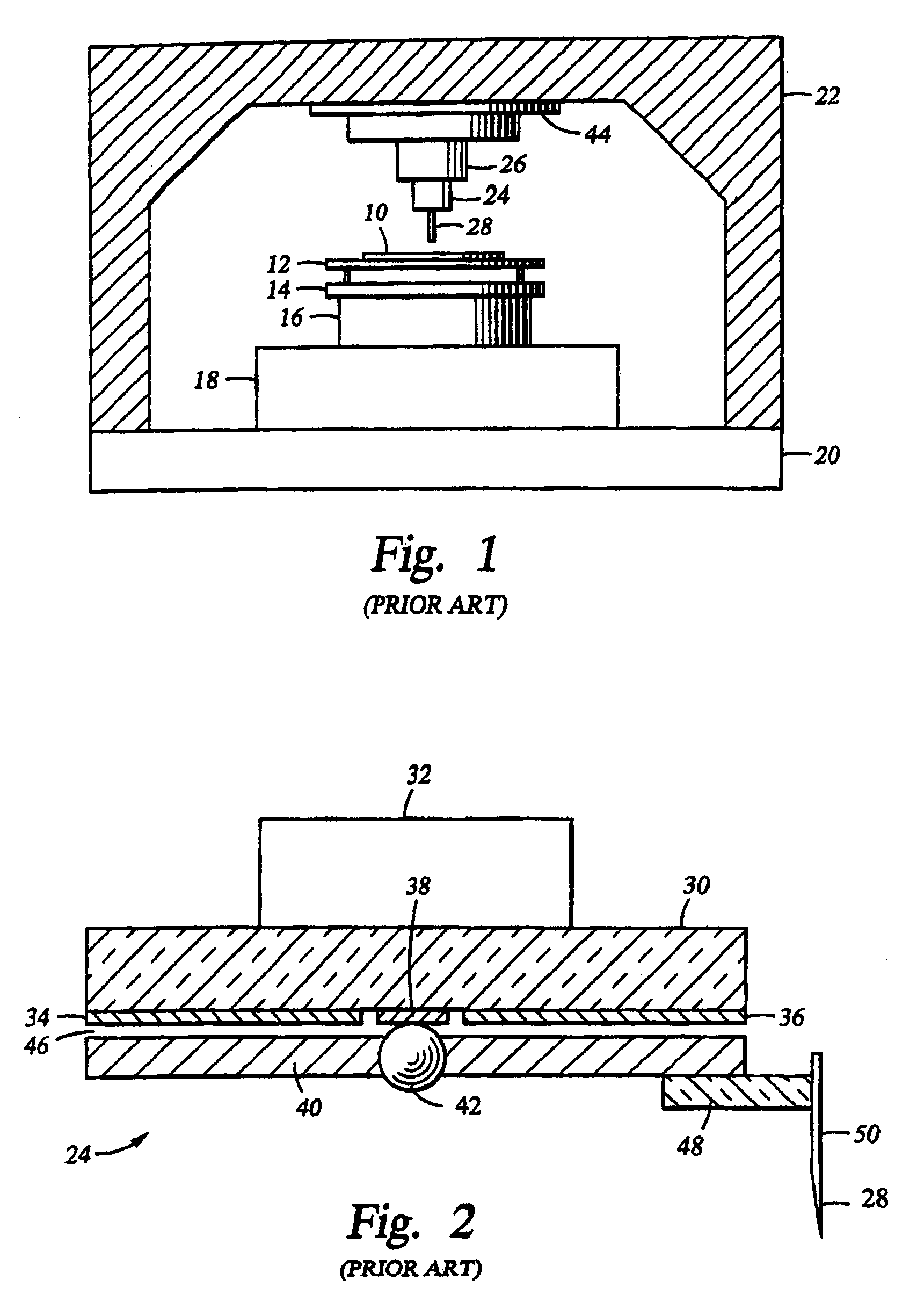
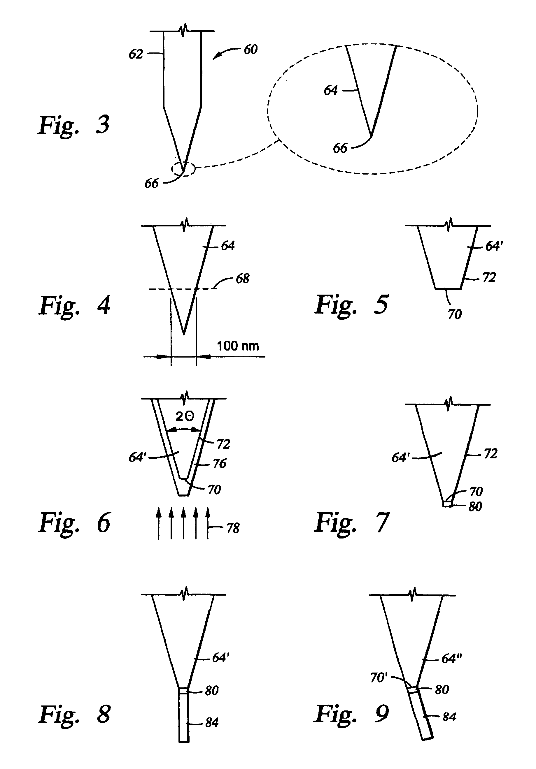
[0033]Preferred embodiments of the invention allow the fabrication of a single carbon nanotube, or a controlled number of nanotubes, on a narrow support structure well suited for easy attachment to a probe of an atomic force microscope (AFM) or other type of microprobe.

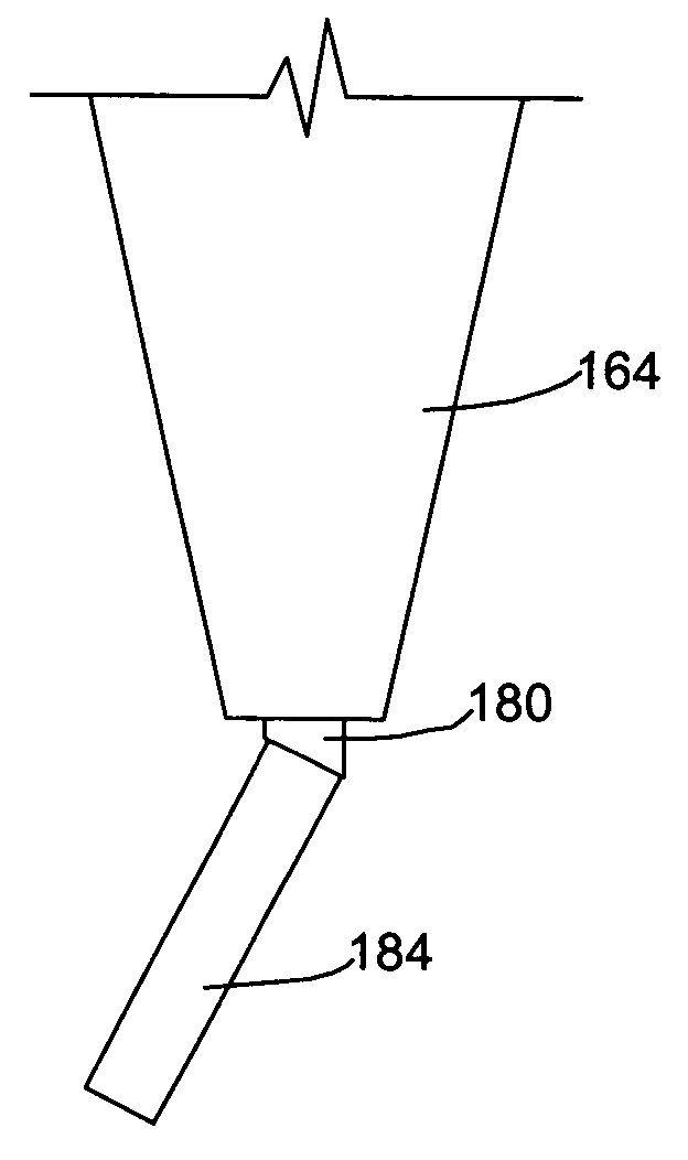
[0034]In one preferred embodiment of the invention described and claimed herein, a probe end is shaped to have sloping sides and a generally flat end, that is, in the shape of sloping mesa. The diameter of the mesa top is preferably in the range of 20 to 300 nm. Nickel or some other material that catalyzes the growth of carbon nanotubes is directionally deposited onto the probe end. Because of the geometry, the thickness of the deposited nickel, as measured from the underlying surface is greater on the mesa top than on the mesa sides. The nickel is then isotropically etched for a time sufficient to remove the nickel from the mesa sides but to leave sufficient nickel on the mesa top to catalyze the growth of a single c...


PUM

PropertyMeasurementUnit
diameteraaaaaaaaaa
widthsaaaaaaaaaa
sizesaaaaaaaaaa

Abstract

A method of fabricating a nanotube probe tip and the resultant probe tip, particularly for use in an atomic force microscope. A moderately sharply peaked support structure has its tip cut or flattened to have a substantially flat end of size of about 20 to 200 nm across. The support structure may be formed by etching a conical end into a silica optical fiber. Nickel or other catalyzing metal such as iron is directionally sputtered onto the flat end and the sloped sidewalls of the support structure. The nickel is anisotropically etched to remove all the nickel from the sidewalls but leaving at least 15 nm on the flat end to form a small nickel dot. A nanotube is then grown with the nickel catalyzing its growth such that only a single nanotube forms on the nickel dot and its diameter conforms to the size of the nickel dot. In another preferred embodiment of the invention, a catalyst material can be directly deposited on to the probe end using charged particle beam deposition, such as electron beam deposition.

Description

[0001]This application is a continuation in part of U.S. patent application Ser. No. 10 / 261,084, filed Sep. 30, 2002, now abandoned which was a continuation of U.S. patent application Ser. No. 09 / 657,428, filed Sep. 8, 2000 and issued Oct. 1, 2002 as U.S. Pat. No. 6,457,350. Both parent applications are hereby incorporated by reference.TECHNICAL FIELD OF THE INVENTION[0002]The invention relates generally to mechanical probe tips such as those used in atomic force microscopy. In particular, the invention relates to a carbon nanotube grown directly on a pointed end of a probe.BACKGROUND AND SUMMARY OF THE INVENTION[0003]Atomic force microscopes (AFMs) have been recently developed for mechanically profiling small features, for example, determining critical dimensions (CDs) of via holes in semiconductor integrated circuits. Such holes have depths of about 1 μm and widths that are being pushed to 180 nm and below. For detailed measurement of the feature, an exceedingly fine probe tip is ...

Claims


Application Information

Patent Timeline
Patent Type & Authority Patents(United States)
IPC IPC(8): G02B5/28B82B3/00C01B31/02G01Q60/24G01Q70/12G01Q70/16
CPCB82Y15/00B82Y30/00B82Y35/00C01B31/0233G01Q70/12B82Y40/00H01J2237/31732C01B2202/36C01B32/162
Inventor LEE, RANDALLMITCHELL, THOMAS OWENMULDERS, JOHANNES JACOBUS LAMBERTUS
Owner FEI CO
Why Eureka
Try Eureka