Nickel (Ni) film annealing side gate graphene transistor preparation method based on reaction of silicon carbide (SiC) and chlorine gas

A graphene and transistor technology, applied in the field of microelectronics, can solve the problems of top-gate GFET mobility decline, graphene film is easily damaged, and energy consumption is large, and achieves fast reaction rate, easy control of thickness, and low porosity Effect

Inactive Publication Date: 2013-05-15
XIDIAN UNIV
View PDF3 Cites 4 Cited by
  • Summary
  • Abstract
  • Description
  • Claims
  • Application Information

AI Technical Summary

Problems solved by technology

The main disadvantages of this method are: complex process, special removal of catalyst is required, large energy consumption and high production cost
They all have certain shortcomings and need further improvement, but this will not affect the prospect of nearly half of the applications of graphene in field effect transistors
In the existing GFET preparation process, graphene needs to be deposited or transferred

Method used


Image

  • Nickel (Ni) film annealing side gate graphene transistor preparation method based on reaction of silicon carbide (SiC) and chlorine gas
  • Nickel (Ni) film annealing side gate graphene transistor preparation method based on reaction of silicon carbide (SiC) and chlorine gas
  • Nickel (Ni) film annealing side gate graphene transistor preparation method based on reaction of silicon carbide (SiC) and chlorine gas

Examples


Embodiment 1

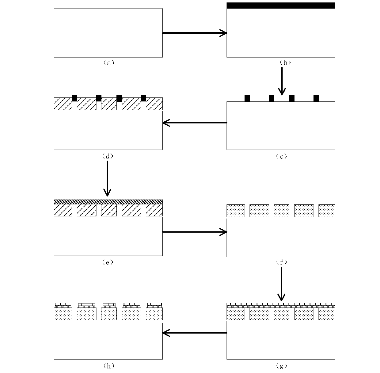
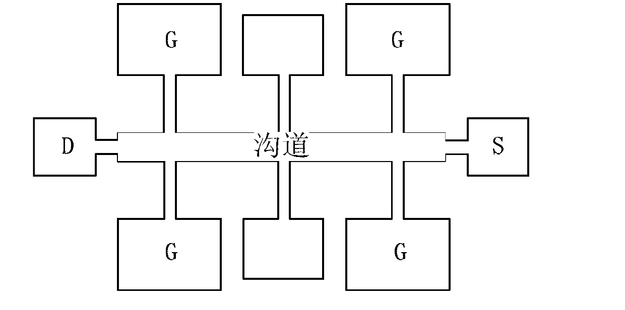
[0039] refer to figure 2 , the steps of making connection type side gate graphene transistor of the present invention are as follows:

[0040] Step 1: Wash the 6H-SiC sample to remove surface contaminants such as figure 2 (a).

[0041] (1.1) Use NH for 6H-SiC substrate 4 OH+H 2 o 2 Soak the sample in the reagent for 10 minutes, take it out and dry it to remove the organic residue on the surface of the sample;

[0042] (1.2) Use HCl+H on the 6H-SiC sample after removing the surface organic residues 2 o 2 The reagent soaked the sample for 10 minutes, took it out and dried it to remove ionic contamination.

[0043] Step 2: Deposit a layer of SiO on the surface of the 6H-SiC sample 2 ,Such as figure 2 (b).

[0044] (2.1) Put the cleaned 6H-SiC sample into the PECVD system, adjust the internal pressure of the system to 3.0Pa, adjust the RF power to 100W, and adjust the temperature to 150°C;

[0045] (2.2) Introduce SiH with flow rates of 30sccm, 60sccm and 200sccm int...

Embodiment 2

[0072] refer to Figure 4 , the present invention makes the steps of the non-connected side-gate graphene transistor as follows:

[0073] Step 1: Clean the 4H-SiC sample to remove surface contaminants such as Figure 4 (a).

[0074] (1.1) Use NH for 4H-SiC substrate 4 OH+H 2 o 2 Soak the sample in the reagent for 10 minutes, take it out and dry it to remove the organic residue on the surface of the sample;

[0075] (1.2) Use HCl+H on the 4H-SiC sample after removing the surface organic residues 2 o 2 The reagent soaked the sample for 10 minutes, took it out and dried it to remove ionic contamination.

[0076] Step 2: Deposit a layer of SiO on the surface of the 4H-SiC sample 2 ,Such as Figure 4 (b).

[0077] (2.1) Put the cleaned 4H-SiC sample into the PECVD system, adjust the internal pressure of the system to 3.0Pa, adjust the RF power to 100W, and adjust the temperature to 150°C;

[0078] (2.2) Introduce SiH with flow rates of 30sccm, 60sccm and 200sccm into the...

Embodiment 3

[0105] refer to Figure 4 , the steps of making non-connected side gate graphene transistor of the present invention are as follows:

[0106] Step A: Use NH on the 6H-SiC substrate substrate 4 OH+H 2 o 2 Soak the sample in the reagent for 10 minutes, take it out and dry it to remove the organic residue on the surface of the sample; use HCl+H 2 o 2 Soak the sample in the reagent for 10 minutes, take it out and dry it to remove ionic contaminants such as Figure 4 (a).

[0107] Step B: Put the cleaned 6H-SiC sample into the PECVD system, adjust the internal pressure of the system to 3.0Pa, adjust the radio frequency power to 100W, and adjust the temperature to 150°C; the flow rates into the system are respectively 30sccm, 60sccm and 200 sccm of SiH 4 , N 2 O and N 2 , the duration is 60min, making SiH 4 and N 2 O reaction, a layer of 0.8 μm thick SiO was deposited on the surface of the 6H-SiC sample 2 mask layer, such as Figure 4 (b).

[0108] Step C: On SiO 2 Th...


PUM

PropertyMeasurementUnit
Thicknessaaaaaaaaaa
Thicknessaaaaaaaaaa

Abstract

The invention discloses a Nickel (Ni) film annealing side gate graphene transistor preparation method based on reaction of silicon carbide (SiC) and chlorine gas, and mainly solves the problem that graphene transistor gate mediums prepared through the prior art result in reduction of migration rates of channel current carriers, and can not effectively control current transferring characteristics. The achieving process of the method is that (1) SiC pattern pieces are cleaned; (2) silicon dioxide (Sio2) masking is deposited on SiC pattern pieces after being cleaned and side gate graphene transistor patterns are photo-etched on the Sio2; (3) the pattern pieces after being photo-etched are placed in a quartz tube and are reacted with chlorine (Cl2) to generate carbon films; (4) the Sio2 masking is removed; (5) a Ni film layer is deposited on an electron beam on carbon film pattern pieces; (6) the carbon film pattern pieces are placed in Argon (Ar) and are generated into side gate graphene in an annealing mode; and (7) a polyether diols (Pd) / Au layer is deposited on the carbon film pattern pieces and is etched into metal contact of the side gate graphene transistor. Side gate graphene transistor manufactured by the Ni film annealing side gate graphene transistor preparation method based on reaction of the SiC and the chlorine gas is high in migration rates of current carriers, capable of accurately controlling channel current of a single transistor and avoiding scattering effect of top gate mediums of a top gate graphene field-effect tube.

Description

technical field [0001] The invention belongs to the technical field of microelectronics, and relates to a method for preparing a semiconductor device, in particular to a method for preparing a Ni film annealed side-gate graphene transistor based on the reaction of SiC and chlorine gas. technical background [0002] As people's demand for high-performance, high-reliability, and low-power equipment increases, more and more attention is paid to the characteristics of devices on integrated circuits. Graphene, a material composed of a two-dimensional hexagonal carbon lattice, has been discovered since 2004 by two scientists, Andre Jem and Kostya Novo, from the University of Manchester, UK, due to its outstanding electrical structural properties. After Love discovered it, it was regarded as a candidate material for the manufacture of high-performance devices. [0003] The preparation method of existing graphene, as application number is 200810113596.0 " method for preparing graph...

Claims


Application Information

Patent Timeline
IPC IPC(8): H01L21/04H01L29/786
Inventor 郭辉张晨旭张玉明张克基雷天民胡彦飞
Owner XIDIAN UNIV
Why Eureka
Try Eureka