Manufacturing method of silicon (Si) substrate upper side grid grapheme field effect tube based on copper (Cu) film annealing

A technology for field effect transistors and manufacturing methods, which is applied in the field of microelectronics, can solve the problems of decreased mobility of top-gate graphene field effect transistors, easy damage of graphene films, etc., and achieves low cost, high safety, and avoids scattering effects Effect

Inactive Publication Date: 2013-06-12
XIDIAN UNIV
View PDF12 Cites 2 Cited by
  • Summary
  • Abstract
  • Description
  • Claims
  • Application Information

AI Technical Summary

Problems solved by technology

They all have certain disadvantages, but this will not affect the application prospects of graphene in field effect transistors
When making graphene field effect transistor GFET in the prior art, the top gate dielectric will introduce more scattering sources, causing front and back scattering. At the same time, during the etching process, the graphene film is also easily damaged, making the top gate graphene field The mobility of effect transistors drops significantly

Method used


Image

  • Manufacturing method of silicon (Si) substrate upper side grid grapheme field effect tube based on copper (Cu) film annealing
  • Manufacturing method of silicon (Si) substrate upper side grid grapheme field effect tube based on copper (Cu) film annealing
  • Manufacturing method of silicon (Si) substrate upper side grid grapheme field effect tube based on copper (Cu) film annealing

Examples


Embodiment 1

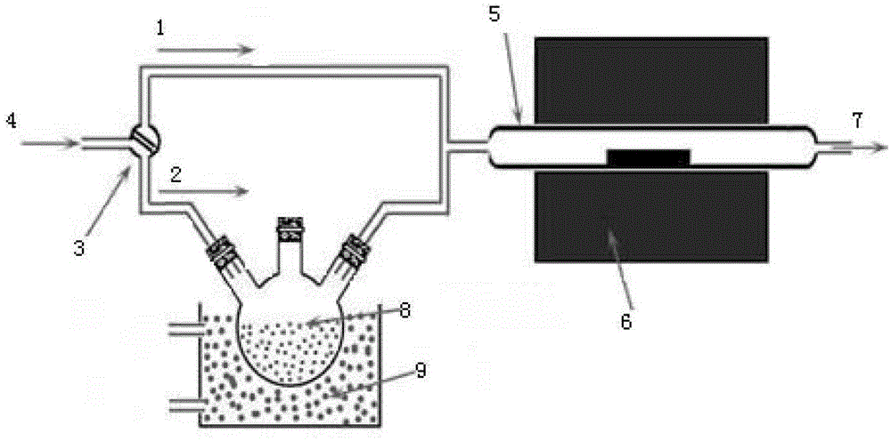
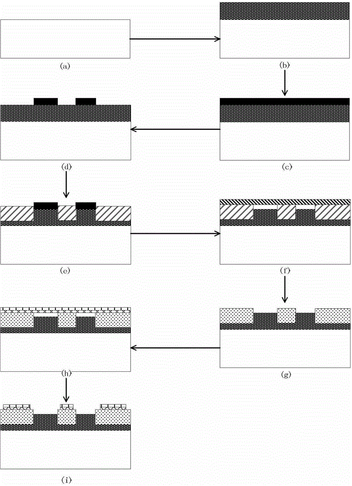
[0033] Step 1: Remove contaminants on the sample surface, such as figure 2 (A).

[0034] Clean the surface of the 4-inch Si substrate substrate, that is, use NH first 4 OH+H 2 O 2 Soak the sample in the reagent for 10 minutes, take it out and dry it to remove the organic residue on the sample surface; then use HCl+H 2 O 2 The reagent is soaked in the sample for 10 minutes, and then dried to remove ionic contaminants.

[0035] Step 2: Growing a carbonized layer.

[0036] Put the Si substrate into the reaction chamber of the CVD system, and vacuumize the reaction chamber to 10 -7 mbar level; again at H 2 In the case of protection, the temperature of the reaction chamber is raised to the carbonization temperature of 900°C; then the flow rate of C is 40ml / min into the reaction chamber 3 H 8 , Grow a carbonized layer on the Si substrate, the growth time is 8min.

[0037] Step 3: Growing 3C-SiC film on the carbonized layer, such as figure 2 (B).

[0038] The temperature of the reaction cham...

Embodiment 2

[0069] Step 1: Remove contaminants on the sample surface, such as figure 2 (A).

[0070] Perform surface cleaning treatment on the 8-inch Si substrate substrate, that is, use NH first 4 OH+H 2 O 2 Soak the sample in the reagent for 10 minutes, take it out and dry it to remove the organic residue on the sample surface; then use HCl+H 2 O 2 The reagent is soaked in the sample for 10 minutes, and then dried to remove ionic contaminants.

[0071] Step 2: Growing a carbonized layer.

[0072] Put the Si substrate into the reaction chamber of the CVD system, and vacuumize the reaction chamber to 10 -7 mbar level. In H 2 In the case of protection, the temperature of the reaction chamber is raised to the carbonization temperature of 1100°C, and then C with a flow rate of 40ml / min is passed into the reaction chamber 3 H 8 , Grow a carbonized layer on the Si substrate, the growth time is 3min.

[0073] Step 3: Growing 3C-SiC film on the carbonized layer, such as figure 2 (B).

[0074] The tempe...

Embodiment 3

[0101] Step A: Perform surface cleaning treatment on the 12-inch Si substrate substrate, that is, use NH first 4 OH+H 2 O 2 Soak the sample in the reagent for 10 minutes, take it out and dry it to remove the organic residue on the sample surface; then use HCl+H 2 O 2 The reagent is soaked in the sample for 10 minutes, and then dried to remove ionic contaminants, such as figure 2 (A).

[0102] Step B: Put the Si substrate into the reaction chamber of the CVD system, and vacuum the reaction chamber to 10 -7 mbar level. In H 2 Under protection, the temperature of the reaction chamber is raised to the carbonization temperature of 1000°C, and then a flow rate of 40ml / min of C is introduced into the reaction chamber 3 H 8 , Grow a carbonized layer on the Si substrate, the growth time is 5min.

[0103] Step C: Raise the temperature of the reaction chamber rapidly to the growth temperature of 1200℃, and pass in SiH with flow rates of 25ml / min and 50ml / min respectively 4 And C 3 H 8 , Perfo...


PUM

PropertyMeasurementUnit
Thicknessaaaaaaaaaa
Thicknessaaaaaaaaaa
Thicknessaaaaaaaaaa

Abstract

The invention relates to a manufacturing method of a silicon (Si) substrate upper side grid grapheme field effect tube based on copper (Cu) film annealing, and mainly resolves the problems that a grapheme field effect tube manufactured in the prior art is severe in carrier scattering and low in migration rate. The manufacturing method includes that (1) a carbonization zone is grown in a Si substrate to serve as transition; (2) 3C-SiC heteroepitaxial growth is carried out under 1100 DEG C-1250 DEG C; (3) SiO2 is deposited on the surface of 3C-SiC; (4) the 3C-SiC reacts with CCl4 in a gaseous state under 800-1000 DEG C to produce a carbon film; (5) a carbon film sample wafer is placed in a moderation hydrofluoric acid solution to remove the SiO2 out of a window; (6) the carbon film sample wafer with the SiO2 removed is placed on a Cu film, and the carbon film sample wafer and the Cu film are then placed in Ar gas at the same time, grapheme is generated under the temperature of 800-1000 DEG C through annealing for 10-25 minutes, and then the Cu film is taken off; and (7) a contact electrode is deposited on the surface of the grapheme, and metallic contact is formed through photoetching. The grapheme field effect tube prepared in the method has high electronic mobility, and effectively avoids carrier scattering effects.

Description

Technical field [0001] The invention belongs to the field of microelectronics technology, and relates to a method for preparing a field effect tube of semiconductor film materials, specifically a method for manufacturing a side gate graphene field effect tube on a Si substrate based on Cu film annealing, which can be used in high-frequency and high-speed circuits . technical background [0002] Two scientists from the University of Manchester, Andre Jem and Kostya Novoslov, discovered graphite flakes in 2004. Since the discovery of this single-layer film structure composed of two-dimensional honeycomb lattices embedded with carbon atoms, graphene has attracted many scholars to invest in this field as a substitute material for future nanoelectronics. Due to its excellent mechanical, thermal, electrical, optical and other properties, graphene has become one of the semiconductor candidate materials that are expected to replace Si. The potential of producing wafer-level graphene fi...

Claims


Application Information

Patent Timeline
IPC IPC(8): H01L21/336H01L29/786
Inventor 郭辉胡彦飞张克基张玉明雷天民张晨旭
Owner XIDIAN UNIV
Why Eureka
Try Eureka