Method for electron beam-initiated coating for application of transmission electron microscopy
a transmission electron microscopy and electron beam technology, applied in the direction of material analysis using wave/particle radiation, instruments, nuclear engineering, etc., can solve the problems of amorphous damage ranging in thickness from 1-10 nanometers, and adversely affecting the quality of tem analysis
- Summary
- Abstract
- Description
- Claims
- Application Information
AI Technical Summary
Benefits of technology
Problems solved by technology
Method used
Image
Examples
Embodiment Construction
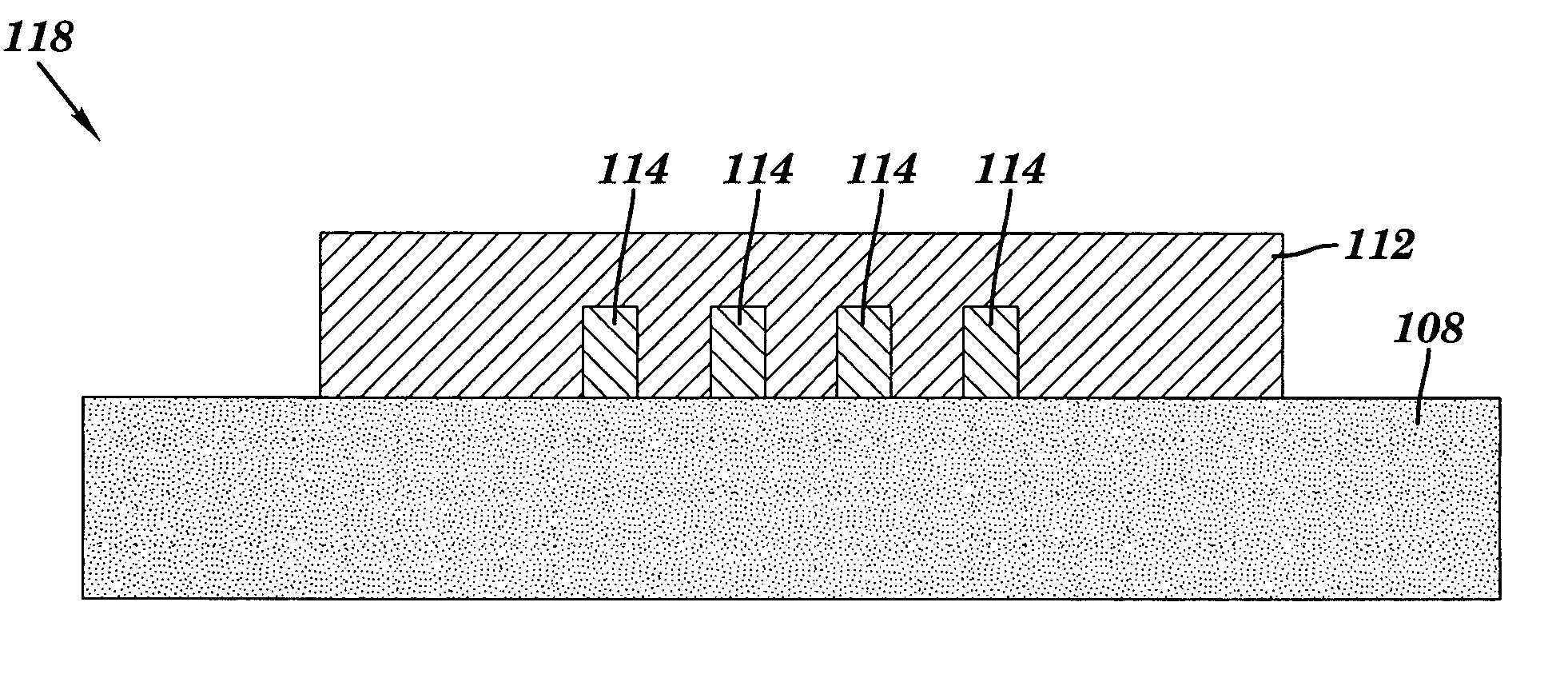
[0016] Disclosed herein is a method for transmission electron microscopy (TEM) sample preparation in which only the area of interest is covered with a conductive metal layer such as platinum. Briefly stated, an initial thickness of conductive metal (e.g., platinum) is locally formed by electron beam (i.e., low-energy) deposition, which protects the topographic features on the surface of the tested sample. Thereafter, this precoated layer may optionally be coated with additional metal formed by ion beam (i.e., high-energy) deposition for increased throughput. In so doing, the damage created on the surface of interest can be minimized.
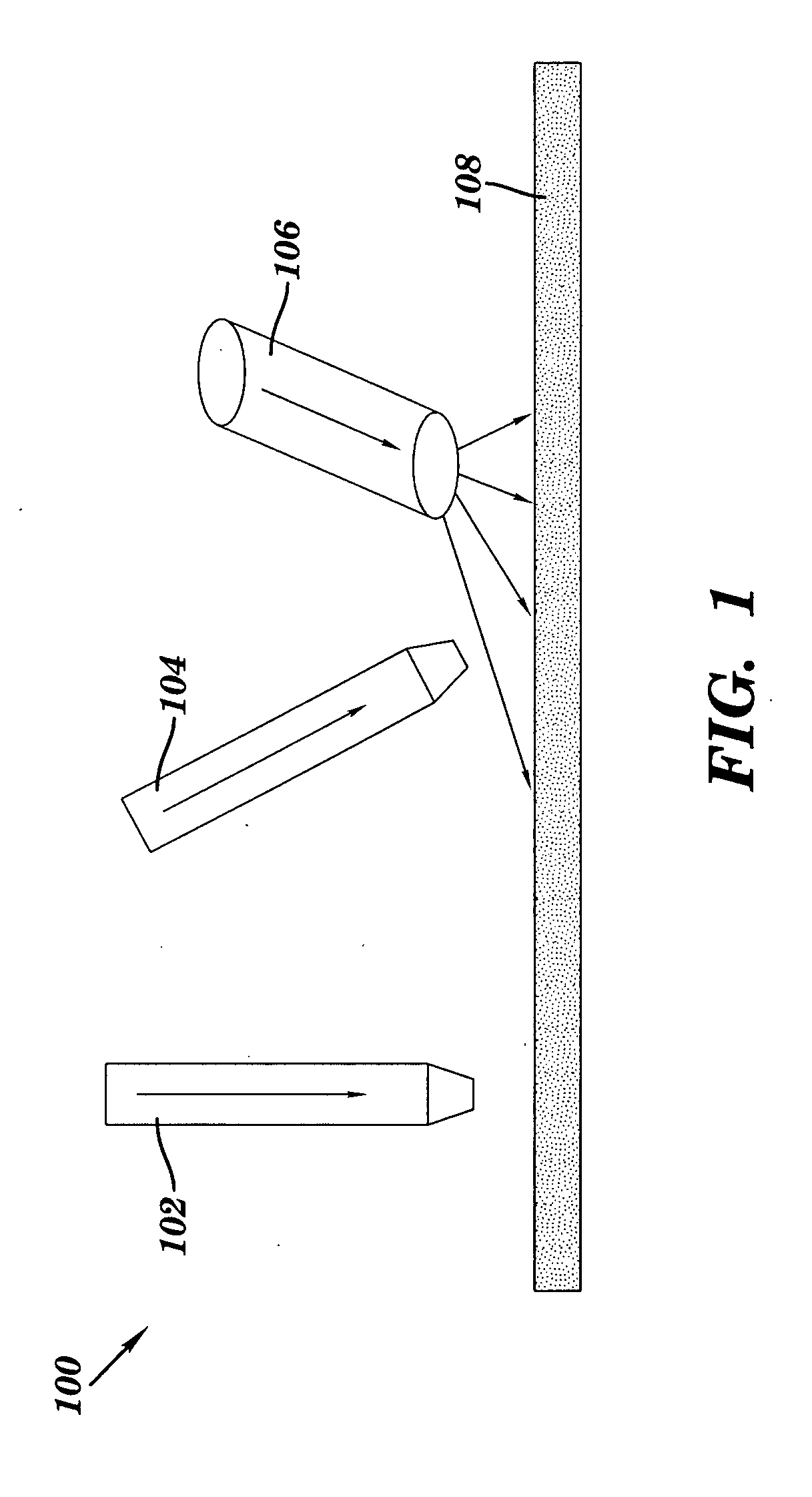
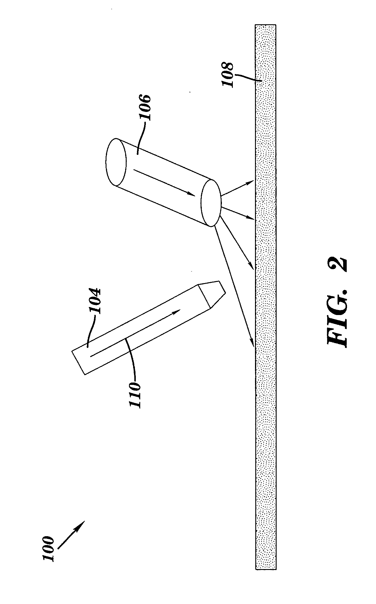
[0017] Referring initially to FIG. 1, there is shown a side sectional view of a tunneling electron microscopy (TEM) preparation system 100 suitable for use in accordance with an embodiment of the invention. System 100 includes a focused ion beam (FIB) column 102, a scanning electron microscope (SEM) column 104 and a precursor delivering tube 106 for sup...
PUM
 Abstract
Description
Claims
Application Information


