
Group-III nitride semiconductor device, production method thereof and light-emitting diode

a technology of nitride semiconductor and semiconductor device, which is applied in the manufacture of semiconductor/solid-state devices, semiconductor devices, electrical devices, etc., can solve the problems of large lattice mismatching between sapphire and ohmic electrodes, low contact resistance of ohmic electrodes, and high crystal density, and achieve low contact resistance.

Inactive Publication Date: 2006-04-25
SHOWA DENKO KK
View PDF9 Cites 7 Cited by
  • Summary
  • Abstract
  • Description
  • Claims
  • Application Information

AI Technical Summary

Benefits of technology

[0016]The present invention has been achieved by taking into account the above-described problems of the prior art, and an object of the present invention is to provide a Group-III nitride semiconductor device comprising an ohmic electrode having a low contact resistance and free from local breakdown.
[0017]As a result of extensive investigations to solve these problems, the present inventors have found that the above-described object is attained by providing a boron phosphide crystal layer having a low dislocation density and excellent crystallinity on a Group-III nitride semiconductor crystal layer, and disposing an ohmic electrode in contact with the surface of the boron phosphide crystal layer. The present invention has been accomplished based on this finding.

Problems solved by technology

However, a large lattice mismatching is present between the sapphire and the AlaGabIncN (0≦a,b,c≦1, a+b+c=1) mixed crystal or the like.
Because of this, an ohmic electrode having sufficiently low contact resistance can hardly be obtained.
Furthermore, the AlaGabIncN crystal layer grown on a sapphire substrate has a problem in that device operating current can leak through dislocation present with a high density in the crystal.
As a result, an ohmic electrode having excellent breakdown voltage cannot be formed.

Method used


Image

  • Group-III nitride semiconductor device, production method thereof and light-emitting diode
  • Group-III nitride semiconductor device, production method thereof and light-emitting diode
  • Group-III nitride semiconductor device, production method thereof and light-emitting diode

Examples


example 1

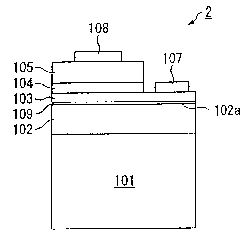
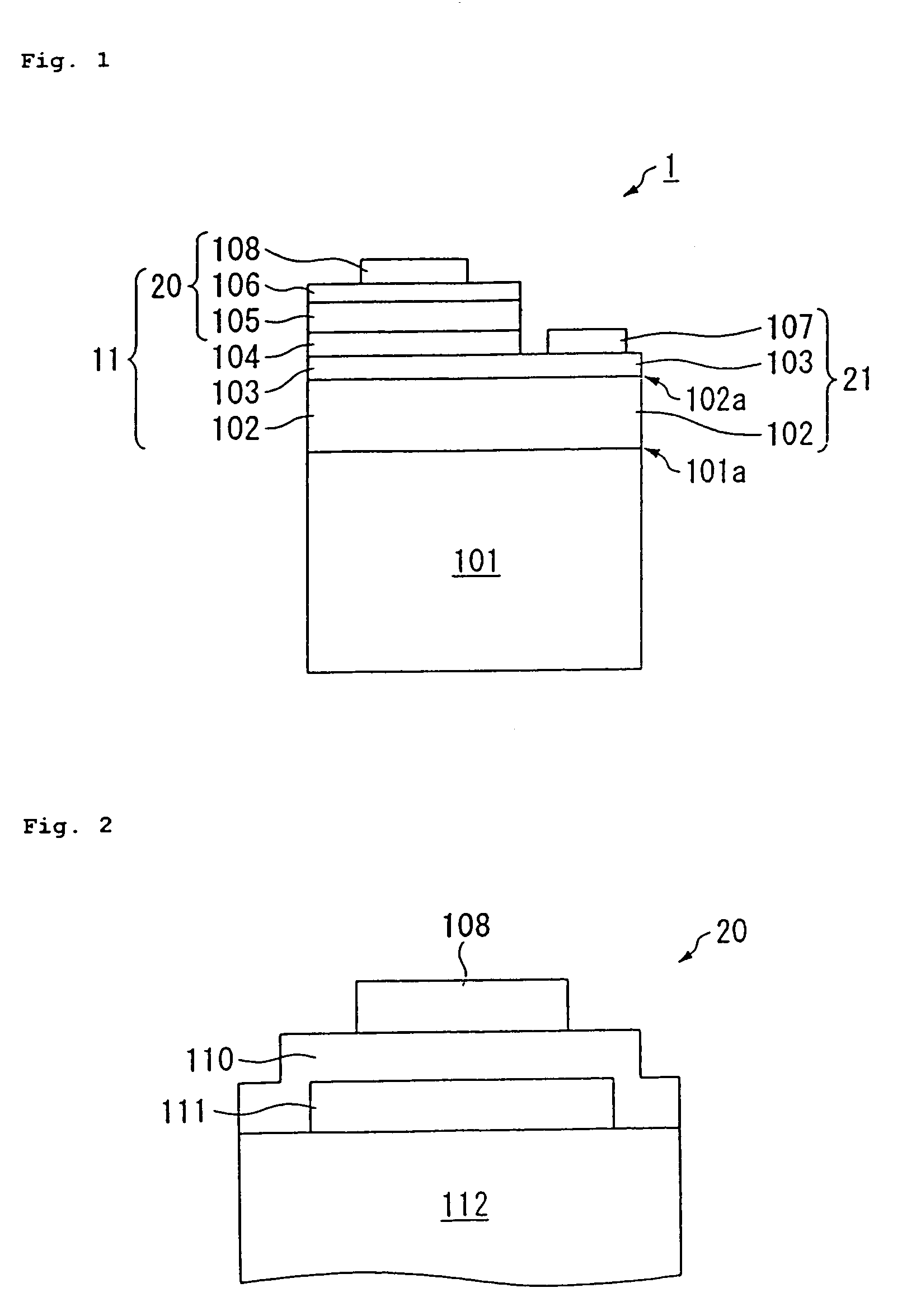
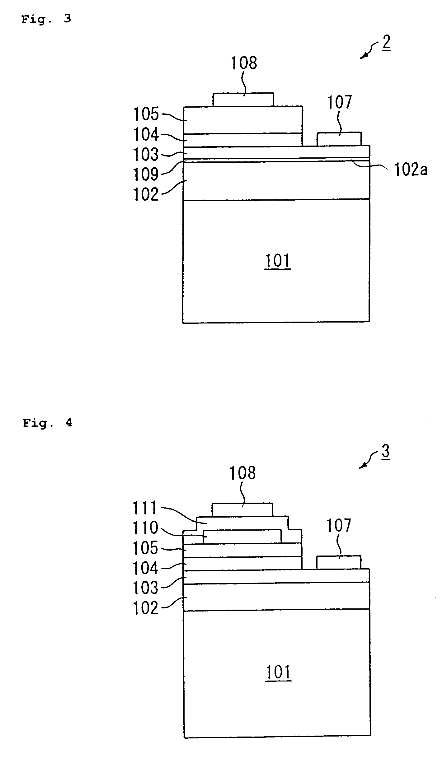
[0047]In this Example, an LED having hetero-junction of a gallium nitride (GaN) layer and a boron phosphide layer was prepared. FIG. 3 shows schematically a cross-sectional structure of LED 2 of this Example. In FIG. 3, the same constituent elements as in FIG. 1 or 2 are shown by the same reference numerals.

[0048]A sapphire having a (0.0.0.1.)-crystal face surface was used as the substrate 101. On the (0.0.0.1.) surface, a lower clad layer 102 constructed with an n-type GaN layer was deposited by an atmospheric-pressure MOCVD method using a trimethyl gallium ((CH3)3Ga) / ammonia (NH3) source system. The gallium nitride (GaN) layer had a {0.0.0.1.}-crystal surface. The thickness of the lower clad layer 102 was 2.8×104 cm (=2.8 μm), and the carrier concentration of the layer 102 was 2×1018 cm−3.

[0049]An undoped amorphous layer 109 containing boron and phosphorus was deposited on the lower clad layer 102. The amorphous layer 109 was deposited at 1,025° C. by a atmospheric-pressure MOCVD ...

example 2

[0061]In this Example, an LED in which both n-type and p-type ohmic electrodes were disposed on a boron phosphide layer was produced.

[0062]FIG. 4 schematically shows a cross-sectional structure view of LED 3 of this Example. The same constituent elements as those in any of FIGS. 1 to 3 are shown by the same reference numerals.

[0063]Under the same conditions as in Example 1, layers 102 to 105 described in Example 1 were sequentially deposited on a (0.0.0.1.)-crystal surface of sapphire substrate 101. Thereafter, an undoped n-type boron phosphide layer 110 was deposited on the p-type upper clad layer 105. The n-type boron phosphide layer 110 was deposited at 850° C. by an atmospheric-pressure MOCVD method using a (C2H5)3B / PH3 / H2 system. The carrier concentration was 1×1019 cm−3 and the layer thickness was 120 nm. After completing growth of the n-type boron phosphide layer 110, only the circular region of the n-type boron phosphide layer 110 underlying beneath the subsequently formed p...


PUM

PropertyMeasurementUnit
band gapaaaaaaaaaa
carrier concentrationaaaaaaaaaa

Abstract

A Group-III nitride semiconductor device including a crystal substrate, an electrically conducting Group-III nitride semiconductor (AlXGaYIn1−(X+Y)N: 0≦X<1, 0<Y≦1 and 0<X+Y≦1) crystal layer vapor-phase grown on the crystal substrate, an ohmic electrode and an electrically conducting boron phosphide crystal layer provided between the ohmic electrode and the Group-III nitride semiconductor crystal layer, the ohmic electrode being disposed in contact with the boron phosphide crystal layer. Also disclosed is a method for producing the Group-III nitride semiconductor device, and a light-emitting diode including the Group-III nitride semiconductor device.

Description

CROSS-REFERENCE TO RELATED APPLICATIONS[0001]This application claims benefit of Provisional Application 60 / 422,121 filed Oct. 30, 2002, incorporated herein by reference, under 35 U.S.C. § 111(b) pursuant to 35 U.S.C. § 119 (e) (1).BACKGROUND OF THE INVENTION[0002]1. Field of the Invention[0003]The present invention relates to a Group-III nitride semiconductor device comprising a crystal substrate having thereon a Group-III nitride semiconductor (AlXGaYIn1−(X+Y)N: 0≦X<1, 0<Y≦1 and 0<X+Y≦1) crysta layer, and an ohmic electrode having a low contact resistance provided thereon via a low dislocation density boron phosphide crystal layer.[0004]2. Related Art[0005]Known examples of a Group-III nitride semiconductor device include a gallium nitride (GaN)-based light emitting diode (LED) or laser diode (LD) and a Schottky contact-type field-effect transistor (MESFET) (see, for example, Patent Document 1). These devices have a stacked structure comprising a functional layer composed ...

Claims


Application Information

Patent Timeline
Patent Type & Authority Patents(United States)
IPC IPC(8): H01L33/00H01L21/00H01L33/14H01L33/32
CPCH01L33/32H01L33/14
Inventor UDAGAWA, TAKASHI
Owner SHOWA DENKO KK
Learn More