Semiconductor device

a technology of semiconductor devices and semiconductors, applied in the direction of semiconductor devices, basic electric elements, electrical appliances, etc., can solve the problems of insufficient cut-off frequency fc, and the method cannot be applied to an avalanche photodiode with an alinas layer or an algaas layer as a multiplication layer, so as to achieve the effect of improving the frequency characteristi

Inactive Publication Date: 2006-05-02
MITSUBISHI ELECTRIC CORP
View PDF1 Cites 12 Cited by
  • Summary
  • Abstract
  • Description
  • Claims
  • Application Information

AI Technical Summary

Benefits of technology

[0015]It is, accordingly, an object of the present invention to provide a semiconductor device having a structure capable of reducing a resistance of a current path when a high frequency current flows.
[0017]A semiconductor device according to the present invention with the construction described above is a semiconductor device constructed with a compound semiconductor, wherein an alternating current component (a high frequency component) of the signal current flows through the second n type layer that can be a layer with low resistance, with a p-n junction capacitance interposed between the first p type layer and the second n type layer, which enables a resistance for a high frequency of a current path to be low, and in turn, enables a high frequency characteristic to be improved.

Problems solved by technology

In the conventional avalanche photodiode shown in FIG. 10, however, a problem has arisen that a cut-off frequency fc cannot be sufficiently high.
This method, however, cannot be applied to an avalanche photodiode with a an AlInAs layer or an AlGaAs layer as a multiplication layer.

Method used


Image

  • Semiconductor device
  • Semiconductor device
  • Semiconductor device

Examples


first embodiment

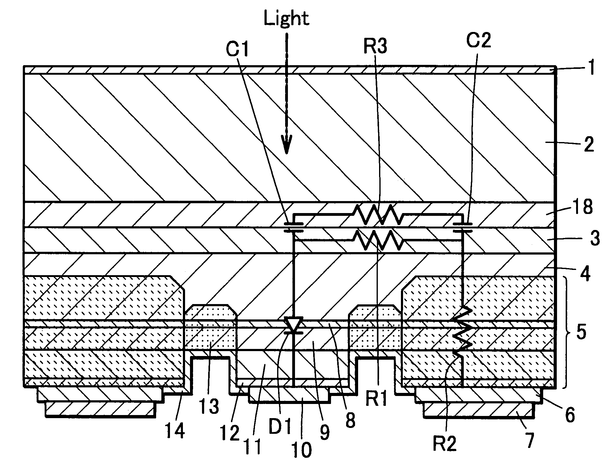
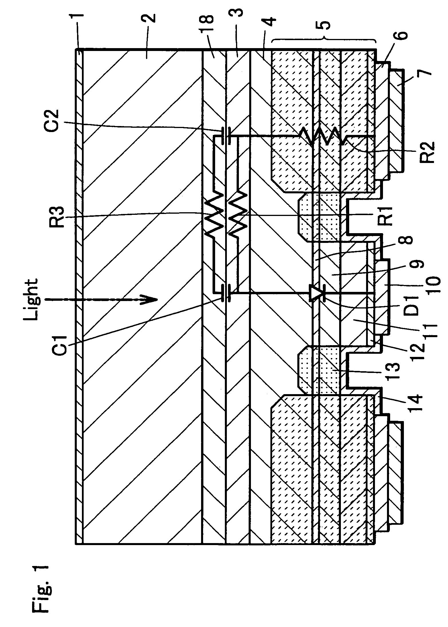
[0031]An optical semiconductor device of a first embodiment according to the present invention is an avalanche photodiode and the avalanche photodiode is constructed in a similar way to that in the conventional example avalanche photodiode of FIG. 10 with the exception that in the conventional example avalanche photodiode of FIG. 10, an n type layer 18 is formed between the semi-insulating InP substrate 2 and the p type layer 3 with a high carrier density.

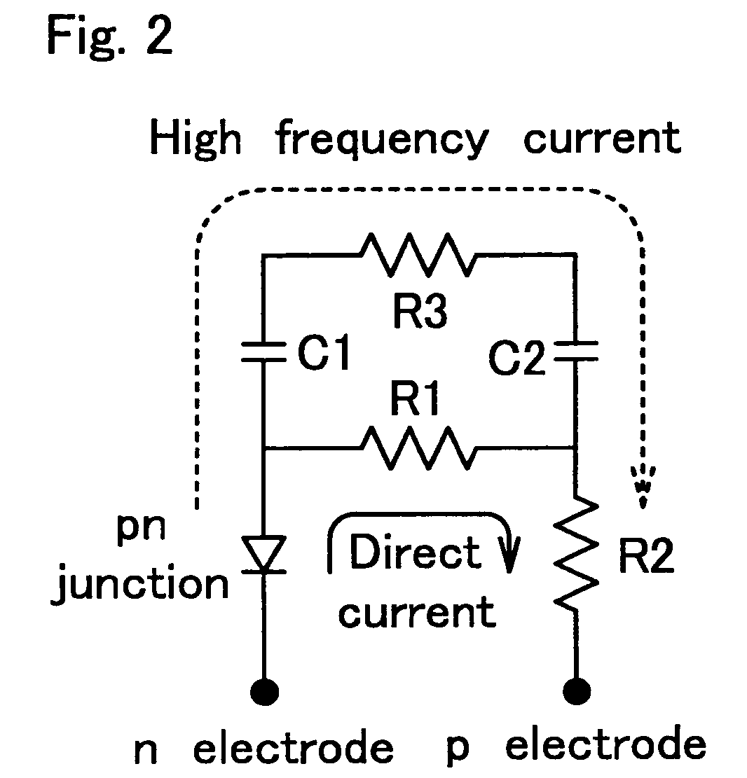
[0032]That is, an equivalent circuit of the avalanche photodiode of the first embodiment is such that in the equivalent circuit of a conventional example avalanche photodiode shown in FIG. 11, as shown in FIG. 2, a series circuit including a capacitance C1, a resistance R3 and a capacitance C2 is connected in parallel to a resistance R1. Herein, in the equivalent circuit of FIG. 2, the capacitance C1 is a pn junction capacitance generated between a p type layer 3 in a light receiving region and an n type layer 18, the resistance R3...

second embodiment

[0045]Then, description will be given of an avalanche photodiode of a second embodiment according to the present invention.

[0046]In the first embodiment, description is given of the case where the p type layer 3 and the n type layer 18 are made of InP, while in the second embodiment, description will be given of an example in which the p type layer 3 and the n type layer 18 are made of another compound semiconductor in an avalanche photodiode with a structure of FIG. 1.

[0047]To be detailed, in the present invention, as the p type layer 3 and the n type layer 18, for example, one selected from the group consisting InAlAs, InGaAsP, AlGaInAs and InGaAs may be used in one layer or in both layers. In a case where the substrate is made of GaAs, GaAs or AlGaAs may be used in one layer or both layers as a structural material.

[0048]In the present invention, to form both or one of the p type layer 3 and the n type layer 18 with a compound semiconductor with a bandgap almost less than 1 eV is ...

third embodiment

[0053]An avalanche photodiode of a third embodiment is similar in fundamental compound semiconductor layer structure to that of the first embodiment with the exception that light comes in through the substrate 2 in the avalanche photodiode of the first embodiment, while in an avalanche photodiode in the third embodiment, light comes in from the side on which the n type side electrode is formed.

[0054]The detailed differences from the first embodiment are the following items.[0055](1) A metal film 22 for device bonding is formed instead of the antireflection film 1 on the rear surface of the InP substrate 2.[0056](2) An annular n type side electrode 10a having an opening for incident light to come in is formed in instead of the n type side electrode 10.[0057](3) An antireflection film 1a is formed on the n type contact layer 12 in the opening of the n type side electrode 10a.

[0058]The avalanche photosensitive diode of the third embodiment is constructed in a similar way to that in th...


PUM


Abstract

A semiconductor device has a structure reducing resistances to a high frequency current. The semiconductor device includes a semi-insulating substrate, a first n-type layer made of a compound semiconductor, and a first p-type layer made of a compound semiconductor in which a signal current flows in a lateral direction, parallel to the semi-insulating substrate. The first p-type layer is sandwiched between the semi-insulating substrate and the first n-type layer. A second n type layer made of a compound semiconductor is between the semi-insulating substrate and the first p type layer. An alternating current component of the signal current flows through the second n type layer.

Description

BACKGROUND OF THE INVENTION[0001]1. Field of the Invention[0002]The present invention relates to a semiconductor device constructed with compound semiconductors, and particularly to a semiconductor device pertaining to a planar avalanche photodiode having a multiplication layer.[0003]2. Description of the Related Art[0004]A conventional planar avalanche photodiode, as shown in, for example, I. Watanabe et al., “Planar-structure Superlattice APDs”, TECHNICAL REPORT OF IEICE., LQE97-79, pp. 69–74 (1997-10), has been of a construction in which formed on one surface of a semi-insulating InP substrate is an anti-reflection film (AR coat) 1, while stacked on the other surface thereof are a p type layer 3 made of InP or AlInAs with a high carrier density, a light absorption layer 4 made of p type InGaAs with a low carrier density, an electric field relaxation layer 8 made of p type InP or AlInAs, a multiplication layer 9 made of AlInGaAs / AlInAs superlattice or AlInAs as a single layer, an ...

Claims


Application Information

Patent Timeline
Patent Type & Authority Patents(United States)
IPC IPC(8): H01L29/732H01L29/861H01L31/107H01L31/0328
CPCH01L31/107
Inventor ISHIMURA, EITARONAKAJI, MASAHARUYAGYU, EIJITOMITA, NOBUYUKI
Owner MITSUBISHI ELECTRIC CORP
Why Eureka
Try Eureka