

Systems and methods for forming metal oxides using alcohols
a metal oxide and alcohol technology, applied in the field of metal oxide layer formation systems and methods, can solve the problems of forming an undesirable siosub>2 /sub>interfacial layer, the layer no longer effectively functions as an insulator, and the performance limit of traditional integrated circuit technology
- Summary
- Abstract
- Description
- Claims
- Application Information
AI Technical Summary
Benefits of technology
Problems solved by technology
Method used
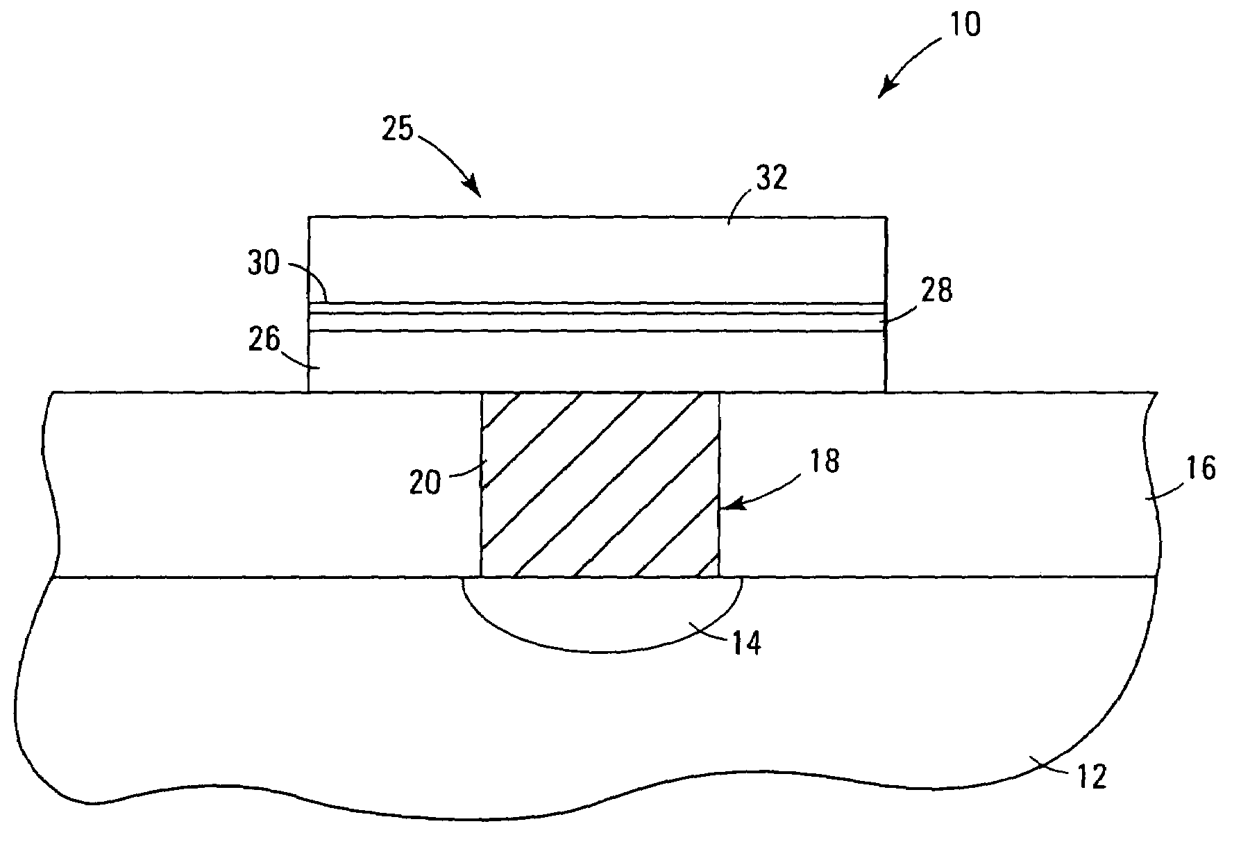
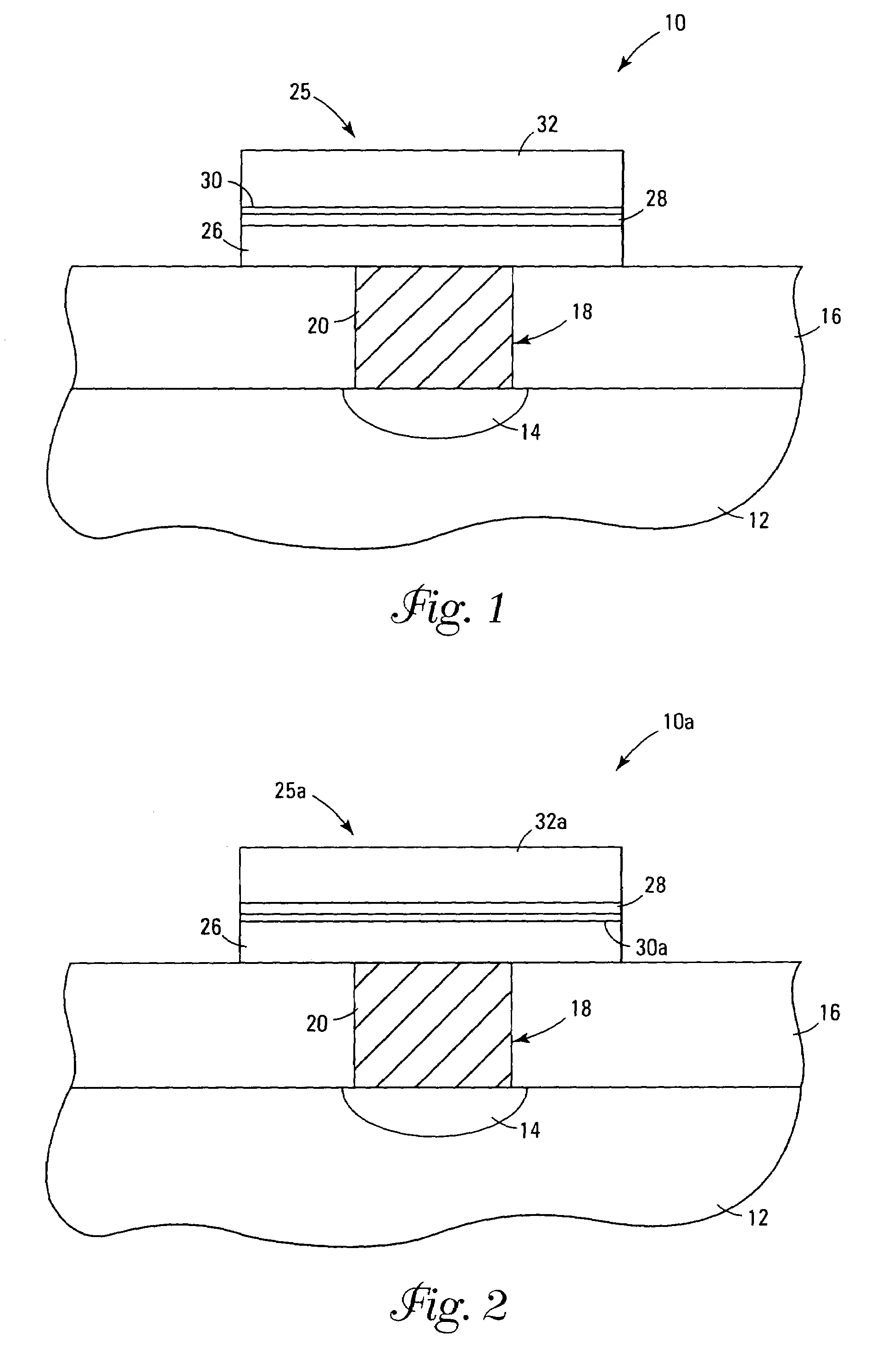
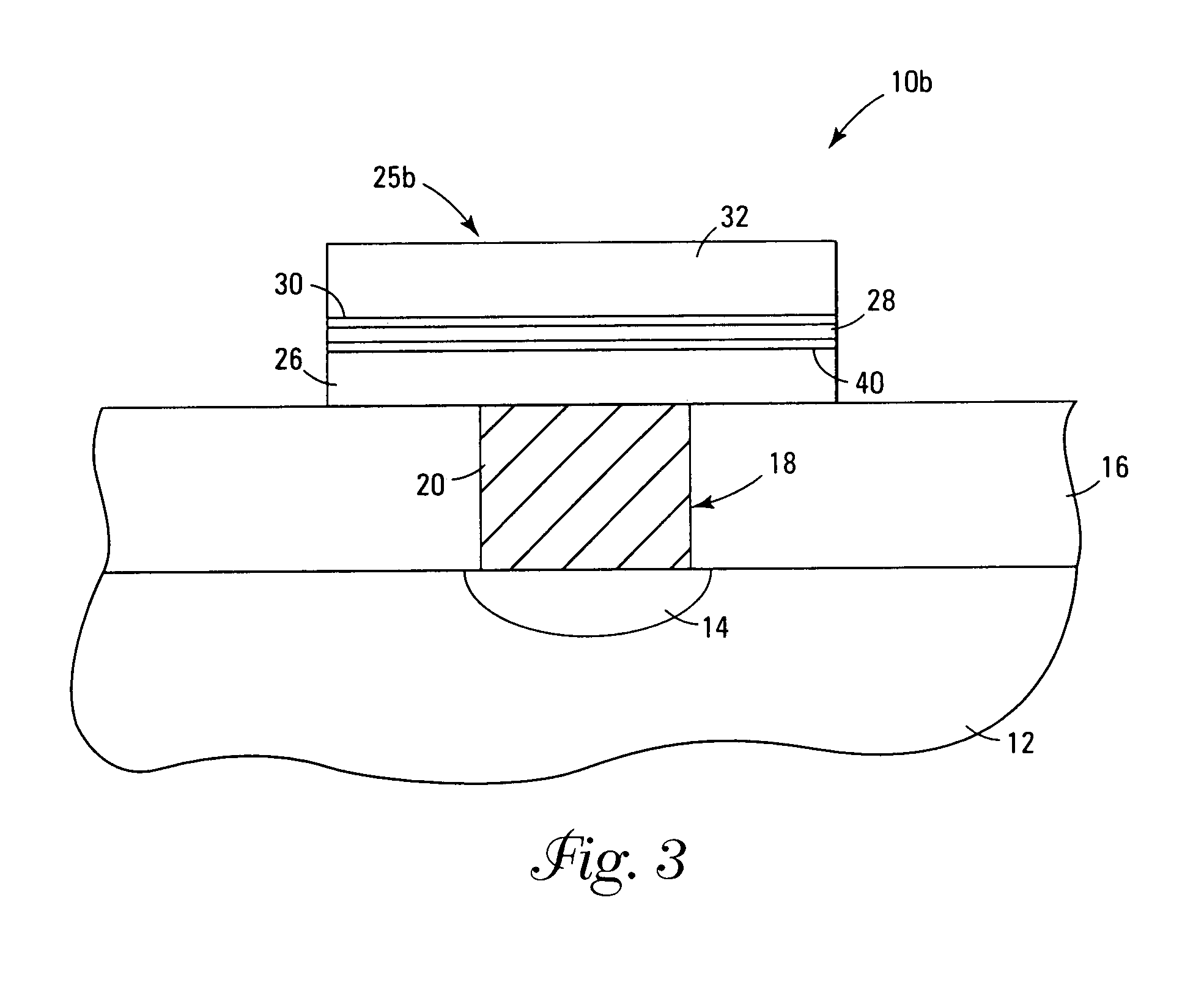
Image

Examples
example 1
Pulsed Chemical Vapor Deposition of TiO2
[0071]A chamber of configuration shown in FIG. 4 was set up with pneumatic valves under computer control to pulse the valves open in sequential manner. Two reservoirs connected to the chamber contained Ti(NMe2)4 (Strem Chemical, Newburyport, Mass.) and isopropyl alcohol (General Chemical, Parsippany, N.J.). The substrate was a silicon wafer having doped poly-silicon as a top layer and was maintained at 220° C. for the deposition.
[0072]Each cycle involved a 5-second pulse of Ti(NMe2)4 and a 5-second pulse of isopropyl alcohol, each separated by a 5-second purge with argon and a 5-second pump down under dynamic vacuum. The precursors were introduced without helium carrier gas, using only a mass flow controller downstream of the isopropyl alcohol reservoir set at 50 sccm. After 400 cycles a TiO2 film 1750 Å thick was obtained. The film contained only titanium and oxygen based on x-ray photoelectron spectroscopy (XPS) analysis, and had no detecta...
example 2
Atomic Layer Deposition of HfO2
[0073]A chamber of configuration shown in FIG. 4 was set up with pneumatic valves under computer control to pulse the valves open in sequential manner. Two reservoirs connected to the chamber contained Hf(NMe2)4 (Strem Chemical, Newburyport, Mass.) and isopropyl alcohol (General Chemical, Parsippany, N.J.). The Hf(NMe2)4 precursor was heated to 40° C. while the isopropyl alcohol remained at ambient. The substrate was a silicon wafer having doped poly-silicon as a top layer and was maintained at 215° C. for the deposition.
[0074]Each cycle involved a 2-second pulse of Hf(NMe2)4 and a 1-second pulse of isopropyl alcohol, each separated by a 5-second purge with argon and a 5-second pump down under dynamic vacuum. The precursors were introduced without helium carrier gas, using only a mass flow controller downstream of the isopropyl alcohol reservoir set at 25 sccm. After 400 cycles a HfO2 film 250 Å thick was obtained. The film contained only hafnium and ...
PUM
| Property | Measurement | Unit |
|---|---|---|
| thickness | aaaaa | aaaaa |
| adsorption energies | aaaaa | aaaaa |
| pressure | aaaaa | aaaaa |
Abstract
Description
Claims
Application Information