Fully-integrated in-plane micro-photomultiplier

a micro-photomultiplier and fully integrated technology, applied in the direction of electron multiplier details, electron discharge tubes, electron multiplier tubes, etc., can solve the problems of dynode and cathode dynode b>110/b> collapse, timely and costly increase of cover thickness, etc., to achieve the effect of simplifying device fabrication

Inactive Publication Date: 2006-05-23
MASSACHUSETTS INST OF TECH
View PDF7 Cites 34 Cited by
  • Summary
  • Abstract
  • Description
  • Claims
  • Application Information

AI Technical Summary

Benefits of technology

[0011]This invention is comprised of a novel design for a fully-integrated micro-photomultiplier and a method for fabricating said device. An all-planar, sub-millimeter-size photomultiplier is proposed which utilizes sub-micron-wide channels for electron amplification. The photocathode, anode, signal collector and electron-amplifying regions are created with standard lithography and microfabrication techniques. The photocathode deposition and vacuum sealing of the device can be accomplished in a final vacuum-deposition step. This invention stems from the discovery that vacuum-deposition sealing of sub-micron-wide channels combined with a novel photomultipier design enable large-scale-integration and simplified device fabrication. This permits the mass production of low-cost, sub-1-mm-size, high-performance photomultipliers, which are suitable for a variety of applications in sensing, imaging and communications.

Problems solved by technology

The size and cost of traditional PMT's precludes their use in such applications as imaging and optical communications.
Unfortunately, the chamber 120 must be under high vacuum, and therefore the covering layer 110 may collapse on the dynodes and cathode unless it is made sufficiently thick.
Increasing the cover thickness will be timely and costly.
This can be a fatal flaw for such a device, since wet etching will ruin most photocathode materials.
The bonding step, required to fasten top and bottom covers, is time consuming and requires careful alignment of the covers to the channels.
The bonding step requires high temperatures, which may also degrade device performance.
The bonding procedure is also susceptible to vacuum leaks, should a small particle exist between the cover and substrate.
Such deep etching can be costly and time consuming.
Again the etching of long narrow holes through the substrate can be time intensive and costly.

Method used


Image

  • Fully-integrated in-plane micro-photomultiplier
  • Fully-integrated in-plane micro-photomultiplier
  • Fully-integrated in-plane micro-photomultiplier

Examples


Embodiment Construction

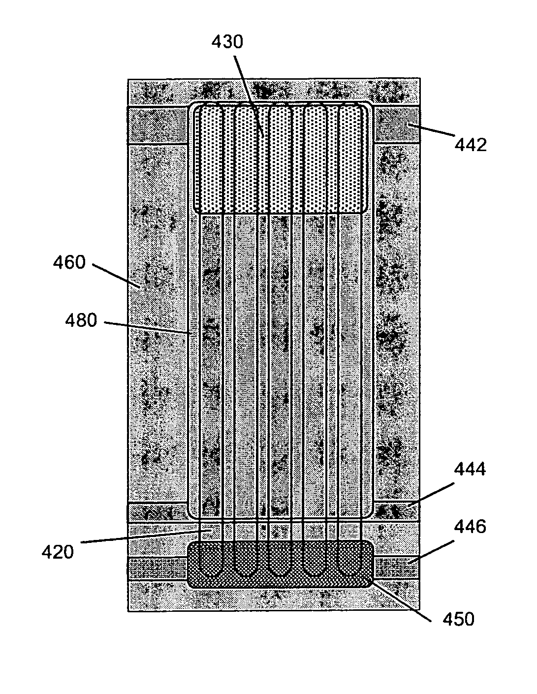
[0017]A planar, fully-integrated micro-photomuliplier device 400 of the invention is shown in FIGS. 4a–4c. FIG. 4a is a top view of the device showing the nanochannels 420, photocathode 430, resistive strip material 480, and buried electrical leads 442, 444 and 446. One electrical lead 442 provides a bias for the photocathode with respect to a second lead 444, which serves as the anode. The final lead 446 makes electrical contact with the signal collector 450, and provides a signal output from the device. For this device the width of the nanochannels is less than 1 micron, and their depth is at least 100 nm. In an exemplary embodiment, their width and depth are each about 200 nm, and the length is typically more than 50 times the width of the nanochannels. Only five channels are shown in the drawing, but the actual device will have tens or hundreds of channels.

[0018]A cut-away end view of the device is shown in FIG. 4b, and a cut-away side view of the device is shown in FIG. 4c. The...


PUM


Abstract

An integrated micro-photomultiplier is disclosed which employs sub-micron-wide channels for electron amplification. These channels are created with standard lithographic and planar-fabrication techniques, and sealed with a vacuum-deposition process. A photocathode, continuous dynode, anode and signal-collector are fabricated along the channels. This photomultiplier design obviates the needs for through-substrate etching, and mechanical assembly of separate layers. Because large-scale-integration techniques can be used to fabricate multiple micro-photomultipliers, significant reductions in device cost and size are expected. The integrated micro-photomultiplier is useful for high-speed, low-light-level optical detection, and may find applications in optical communications, visible or infrared imaging, and chemical or biological sensing.

Description

[0001]This invention was made with government sponsorship under Contract No. N66001-00-1-8932 awarded by the U.S. Navy. The government has certain rights in the invention.BACKGROUND OF THE INVENTION[0002]Conventional photomultipliers (PMTs) are large (>1 cm3), stand-alone devices that exhibit high gain for low-light-level detection. The best PMTs can detect a single photon, and some PMTs have response times of 1 nanosecond or less. The costs of conventional PMTs have fallen to about $500 per device. To date, PMTs have not been integrated onto chips, even though at least two designs have been proposed (see U.S. Pat. No. 5,568,013 and U.S. Pat. No. 5,264,693). The size and cost of traditional PMT's precludes their use in such applications as imaging and optical communications.[0003]Ultrasensitive optical detection is desirable for optical sensors, spectral analysis, imaging, optical receivers and fluorescent microscopy. For example, some recent efforts to develop DNA-sequencing chi...

Claims


Application Information

Patent Timeline
Patent Type & Authority Patents(United States)
IPC IPC(8): H01J43/04
CPCH01J43/246H01J43/04
Inventor GOODBERLET, JAMES G.MOORTHY, VEMURA H. S.
Owner MASSACHUSETTS INST OF TECH
Why Eureka
Try Eureka