Lumped Raman amplification structure for very wideband applications

Inactive Publication Date: 2006-05-30
CISCO TECH INC
View PDF35 Cites 7 Cited by
  • Summary
  • Abstract
  • Description
  • Claims
  • Application Information

AI Technical Summary

Benefits of technology

[0008]Embodiments of the present invention provide improved lumped Raman amplification systems. A lumped Raman amplification structure provides optimized efficiency, low noise figure over a range of gain settings, and a high saturation threshold. Responsibility for amplifying different portions of the spectrum is divided among multiple stages. In one particular implementation, two outer stages amplify a first band and two inner stages amplify a second band. The two inner stages also apply a small amount of amplification to the first band. A modification improves noise figure in the second band by adding some amplification in the second band to the first stage.

Problems solved by technology

Available optical fiber bandwidth has been only partially utilized in high capacity optical transmission due to lack of applicable optical amplifier technologies to overcome fiber losses in the wavelength range 1300 nm to 1650 nm.
A disadvantage of Raman amplification is poor power conversion efficiency in comparison to EDFAs.
The use of multiple EDFAs raises the cost of that approach to an unacceptable level.
When bandwidths are very wide, (e.g., >50 nm) and the number of channels is also large, input amplifier power will be very large giving rise to saturation difficulties with EDFA technology.
However, the saturation advantage of lumped Raman amplifier technology in this situation is limited due to interactions among multiple pump signals that are used to establish the very broad amplification bandwidth.
In particular, for bandwidths greater than 60 nm, the combination of pump-to-pump interactions and high input power leads to uncontrollable saturation effects unless effective countermeasures are implemented.
These approaches add undesired complexity.
There may be rapid changes in optical network configuration over time due to traffic variations leading to addition and deletion of channels from the channel grid.

Method used


Image

  • Lumped Raman amplification structure for very wideband applications
  • Lumped Raman amplification structure for very wideband applications
  • Lumped Raman amplification structure for very wideband applications

Examples


Embodiment Construction

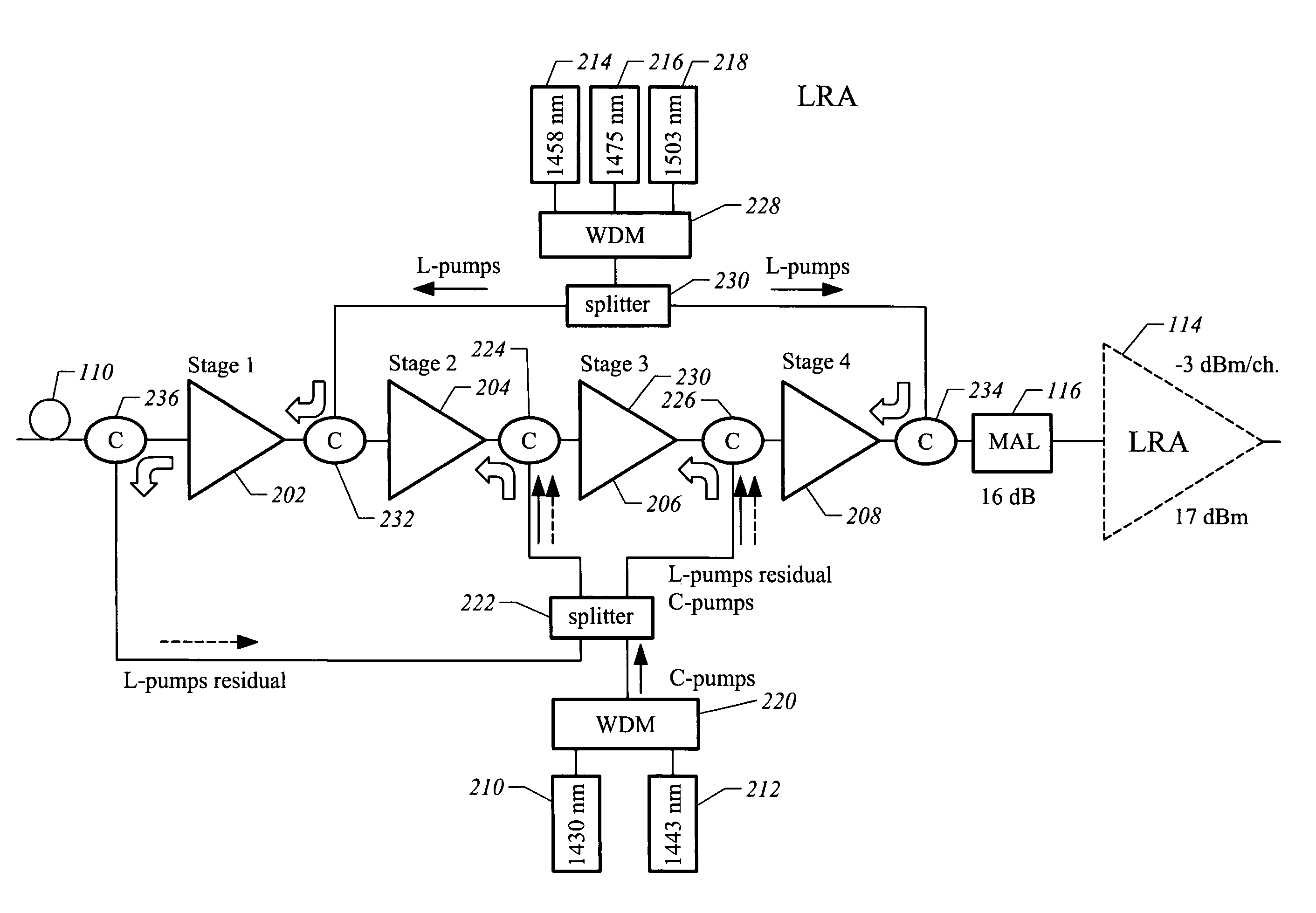
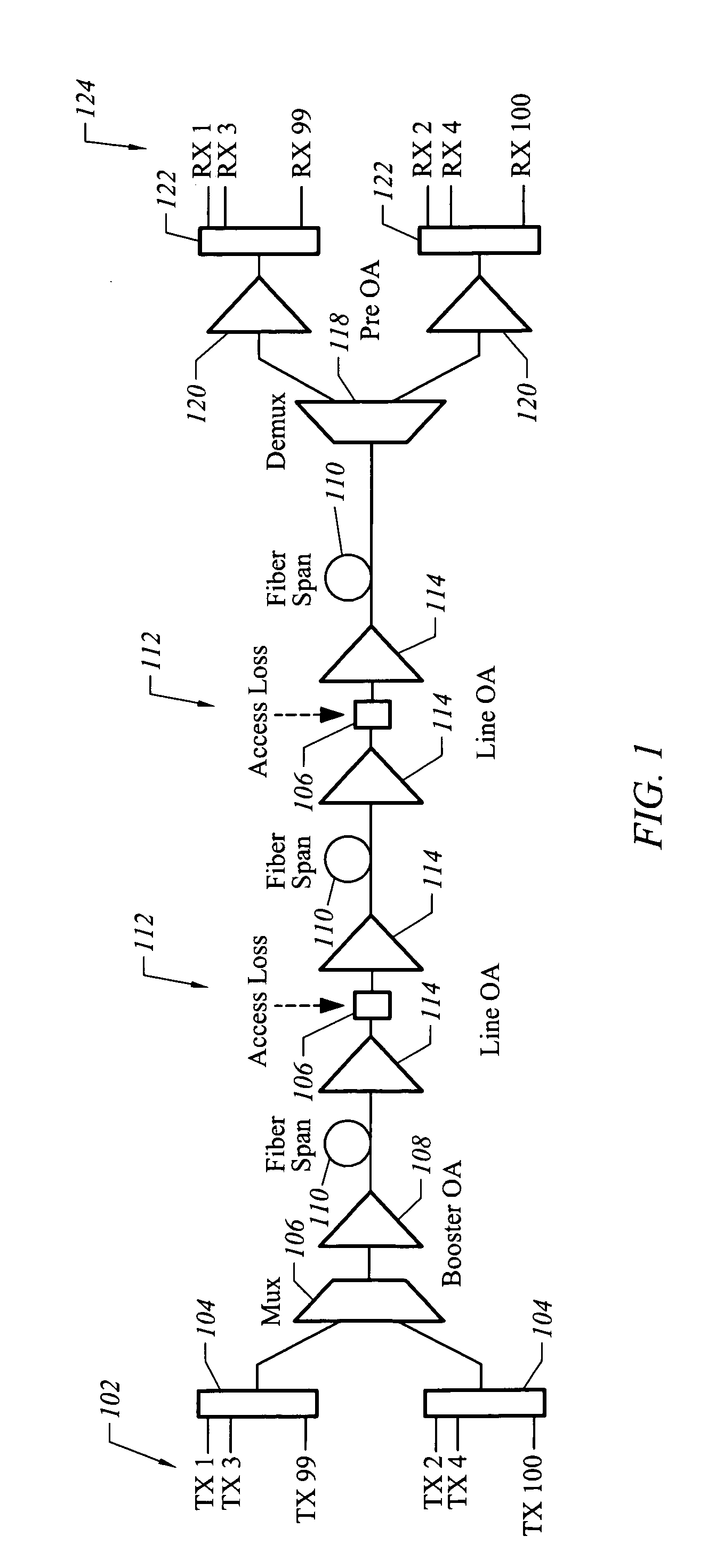
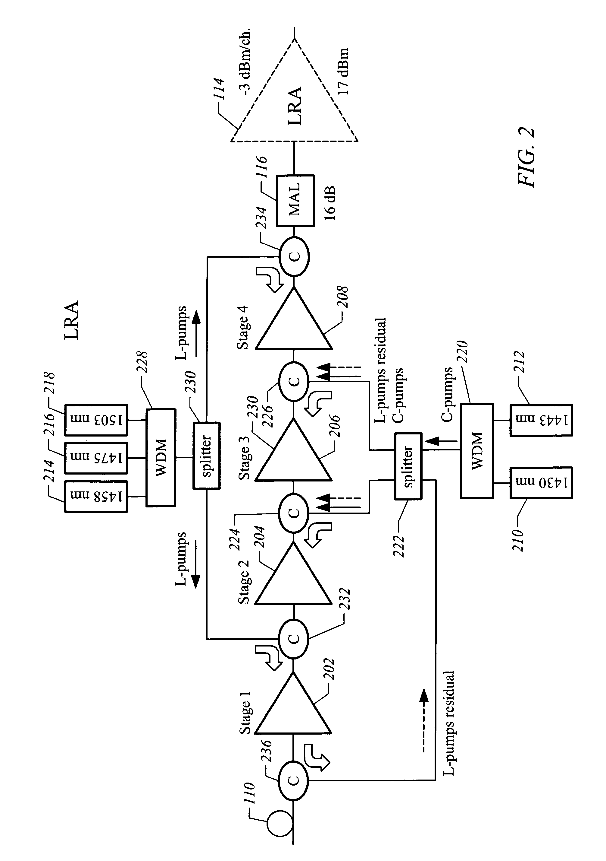
[0018]The present invention will be described with reference to a representative optical wavelength division multiplexing (DWM) system architecture. In the representative architecture there are 100 channels or wavelengths spaced 100 GHz apart. The channels are found in the wavelength range of 1530 nm to 1610 nm. Each channel carries a 10 Gbps transmission. The optical signal to noise ratio (OSNR), at the receiver, should be greater than 14 dB over 0.5 nm bandwidth.

[0019]Single mode fiber (SMF) is used. The link consists of a transmitter site, a receiver site, a series of optical amplification sites, and a series of fiber spans between the sites. Some possible span configurations include seven spans of 14 dB loss (7×14) 5×20, 2×26, 1×31. In each case the amplifier sites provide gain to compensate for the losses of the preceding span. The overall maximum link length before regeneration of the optical signal from recovered data is considered in this example to be approximately 400 Km.

[...


PUM


Abstract

Improved lumped Raman amplification systems are disclosed. A lumped Raman amplification structure provides optimized efficiency, low noise figure over a range of gain settings, and a high saturation threshold. Responsibility for amplifying different portions of the spectrum is divided among multiple stages. In one particular implementation, two outer stages amplify a first band and two inner stages amplify a second band. The two inner stages also apply a small amount of amplification to the first band. A modification improves noise figure in the second band by adding some amplification in the second band to the first stage.

Description

BACKGROUND OF THE INVENTION[0001]The present invention relates to optical networking and more particularly to systems and methods for optical amplification.[0002]Available optical fiber bandwidth has been only partially utilized in high capacity optical transmission due to lack of applicable optical amplifier technologies to overcome fiber losses in the wavelength range 1300 nm to 1650 nm. Lumped Raman amplifiers allow the designer to adjust the spectral position and spectral width of the amplification region to optimally account for channel capacity, channel spacing, and transmission fiber type. Lumped Raman amplification also provides important advantages in that the same fiber can provide gain and dispersion compensation simultaneously while maintaining low noise figure in comparison to standard EDFA (Erbium-doped fiber amplifier) technology.[0003]A disadvantage of Raman amplification is poor power conversion efficiency in comparison to EDFAs. For example, a typical lumped Raman ...

Claims


Application Information

Patent Timeline
IPC IPC(8): H04B10/12
CPCH04B10/2916H01S3/094015H01S3/094096H01S3/302H01S3/0677H01S3/06758H01S3/06766H01S2301/04
Inventor MELI, FAUSTOPASTORELLI, ROSANNACASTAGNETTI, ROBERTA
Owner CISCO TECH INC
Why Eureka
Try Eureka