

Method for cleaning deposition chambers for high dielectric constant materials
a technology of dielectric constant materials and deposition chambers, which is applied in the direction of cleaning using liquids, lighting and heating apparatuses, furnaces, etc., can solve the problems of high leakage current and device failure, no process details for plasma cleaning of ald chambers, and material electric breakdown and no longer providing insulation, etc., to achieve high resolution, high resolution, and high resolution
- Summary
- Abstract
- Description
- Claims
- Application Information
AI Technical Summary
Benefits of technology
Problems solved by technology
Method used
Image

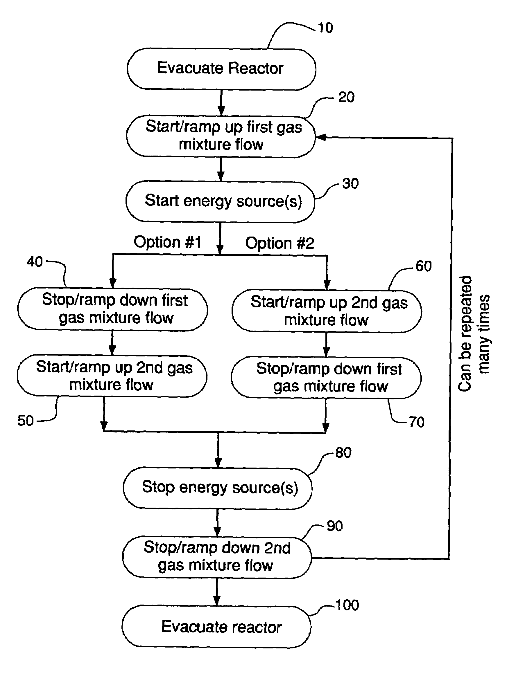
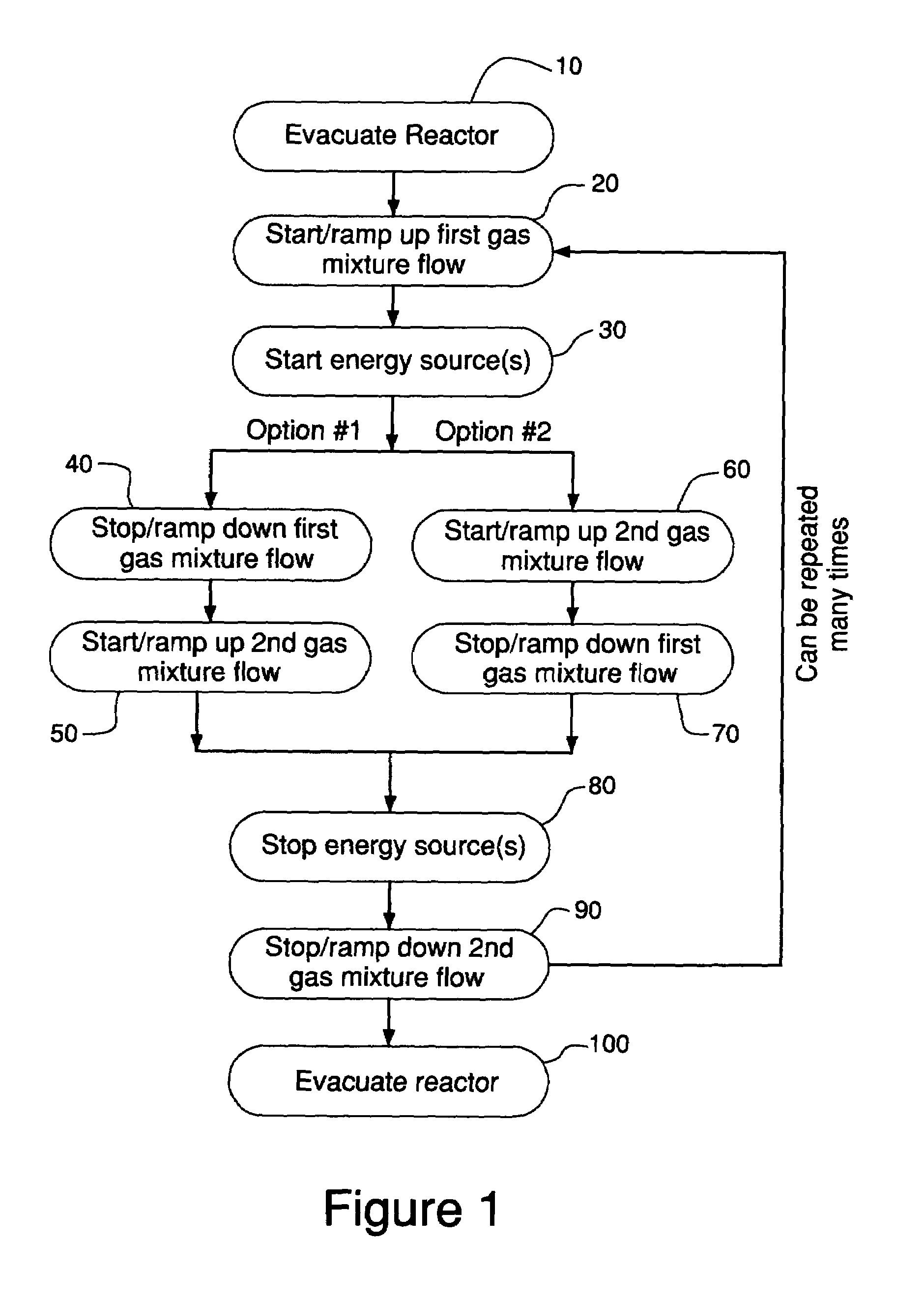
Examples
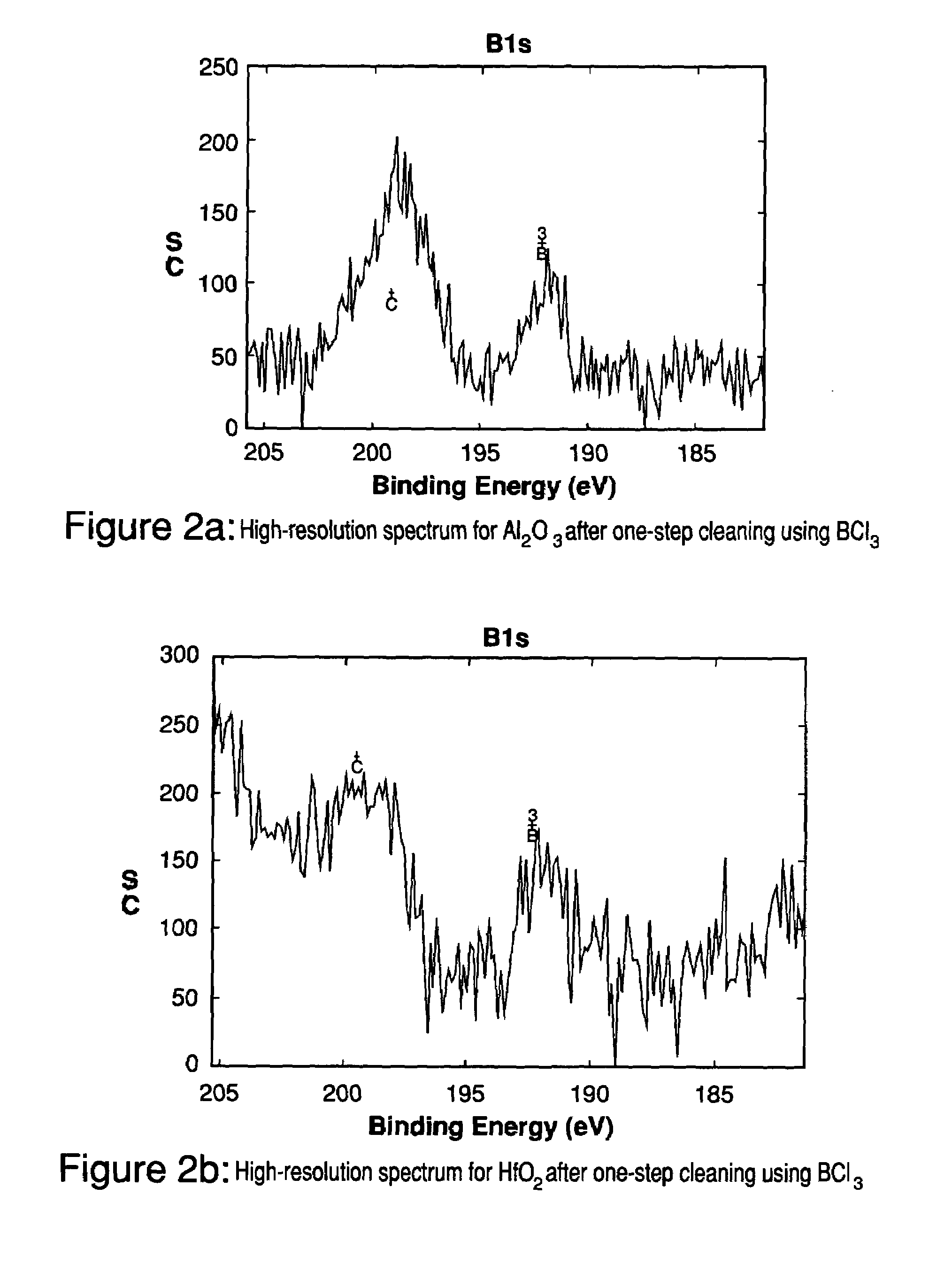
example 1
One-Step Cleaning Using BCl3
[0054]One-step cleaning experiments have been conducted for both Al2O3 and HfO2 samples. Experimental conditions and results are listed in Table 12. The high-resolution XPS spectra for B1s are shown in FIGS. 2a and 2b. After the BCl3 plasma etching step, there were boron residues remaining on the surfaces of both Al2O3 and HfO2 samples and the boron residues existed as B3+. The etch rate for Al2O3 and HfO2 was 4.1 nm / min and 5.4 nm / min, respectively.
example 2
One-Step Cleaning Using a Mixture of BCl3 and NF3
[0055]This present example was conducted to determine if a mixture of BCl3 and NF3 could eliminate the boron residues. Experimental conditions and results are provided in Table 12. High-resolution XPS spectra for B1s are shown in FIGS. 3a and 3b. As Table 12 illustrates, there was still boron residues remaining on the surfaces of both Al2O3 and HfO2 samples.
example 3
Two-Step Cleaning
[0056]In the present experiment, BCl3 was used as the reactive agent in the first gas mixture and a mixture of NF3 and He was used as the reactive agent for the second gas mixture. Table 12 provides the experimental conditions and results. FIGS. 4a and 4b shows the high-resolution XPS spectra for B1s. Within 1 minute for the HfO2 sample and 3 minutes for the Al2O3 sample, the boron residues were removed to a level below the minimum detection limit (0.1 atom %) of the XPS instrument. The Al2O3 sample still had a boron residue of 0.2 atom % when the clean time for the second step was 1 minute.
[0057]
TABLE 12SecondProcessSecondBoronPowerFirst ProcessGas FlowStepResidueDensityGas Flow(sccm)Clean(atomicEx.Material(W / cm2)Press. (mTorr)(sccm)NF3HeTime%)1Al2O30.55500 10 (BCl3)0000.9%1HfO20.55500 10 (BCl3)0000.8%2Al2O30.5550011.25 (BCl3);0000.8% 3.75 (NF3)2HfO20.5550011.25 (BCl3);0000.6% 3.75 (NF3)3Al2O30.55500 10 (BCl3)8.749.333HfO20.55500 10 (BCl3)8.749.31
PUM
| Property | Measurement | Unit |
|---|---|---|
| dielectric constant | aaaaa | aaaaa |
| temperature | aaaaa | aaaaa |
| pressure | aaaaa | aaaaa |
Abstract
Description
Claims
Application Information