Method and device for thermal treatment of substrates

a substrate and thermal treatment technology, applied in the field of methods and devices for thermal treatment of substrates, can solve the problems of difficult separation of background radiation emitted by heat lamps from radiation emitted by heat lamps, rapid decrease of radiation emitted from the background, and unfavorable signal (radiation emitted from the wafer) to the background, so as to achieve reliable heating of the substrate, the effect of maximum heating rate of the wafer and careful yet rapid heating of the structure wafer

Inactive Publication Date: 2006-06-06
BEIJING E TOWN SEMICON TECH CO LTD +1
View PDF13 Cites 22 Cited by
  • Summary
  • Abstract
  • Description
  • Claims
  • Application Information

AI Technical Summary

Benefits of technology

[0024]Thus, as a function of the wafer temperature, the present invention permits the ratio of the radiations of the first and second radiation sources to be controlled or regulated in such a way that it does not fall below a prescribed signal-to-background ratio for the measurement arrangement via the radiation detector, and hence, for example for silicon wafers, over the entire temperature range of about 250° C. to 600° C. a reliable temperature measurement is possible at a maximum heating-up rate of the wafer. In this connection, the radiation contribution of the second radiation source to the overall radiation contribution can be a function of the wafer temperature, ranging from about 1% at about 200° C. of the wafer to 50% at about 600° C. of the wafer. The control or regulation furthermore makes it possible for the contribution of the second radiation source to exceed 50% and for the wafer to be heated exclusively by the second radiation source. This can be advantageous in particular at temperatures over 600° C., especially with structured wafers in order to enable a careful yet rapid heating-up of structured wafers, for example from the back side of the wafer, so that even at heating rates of 300° C./s, the structures on the wafer are not destroyed.
[0025]If the first and second radiation sources are respectively disposed on different sides of the substrate, the substrate can advantageously be heated up on both sides as a function of its temperature and of its optical characteristics, so that one does not fall below a prescribed signal-to-background ratio of the measurement arrangement for the determination of the substrate temperature. Thus, even at low temperatures, a reliable heating-up of the substrate at maximum heating rates is ensured, whereby it is also possible to regulate the heating-up rate with the aid of the still acceptable signal-to-background ratio. This ensures that in particular in the range of low temperatures, the measurement arrangement via the radiation detector itself operates reliably at high heating-up rates of the substrate, and the substrate is increasingly heated from both sides as the temperature increases. The aforementioned advantages and possibilities of the present invention are achieved in particular by the modulation of th...

Problems solved by technology

Furthermore, due to the possibility of the rapid heating and the rapid cooling off, the RTP units provide for the production of new wafer or component characteristics that could not be achieved with conventional furnace processes.
However, the temperature measurement based on pyrometers has the problem that there is present in the process or reflector chamber a strong radiation field that makes a differentiation of the radiation emitted from the wafer from the background radiation emitted from the h...

Method used


Image

  • Method and device for thermal treatment of substrates
  • Method and device for thermal treatment of substrates
  • Method and device for thermal treatment of substrates

Examples


Embodiment Construction

[0033]The invention will be explained in greater detail subsequently with the aid of preferred embodiments of the present invention.

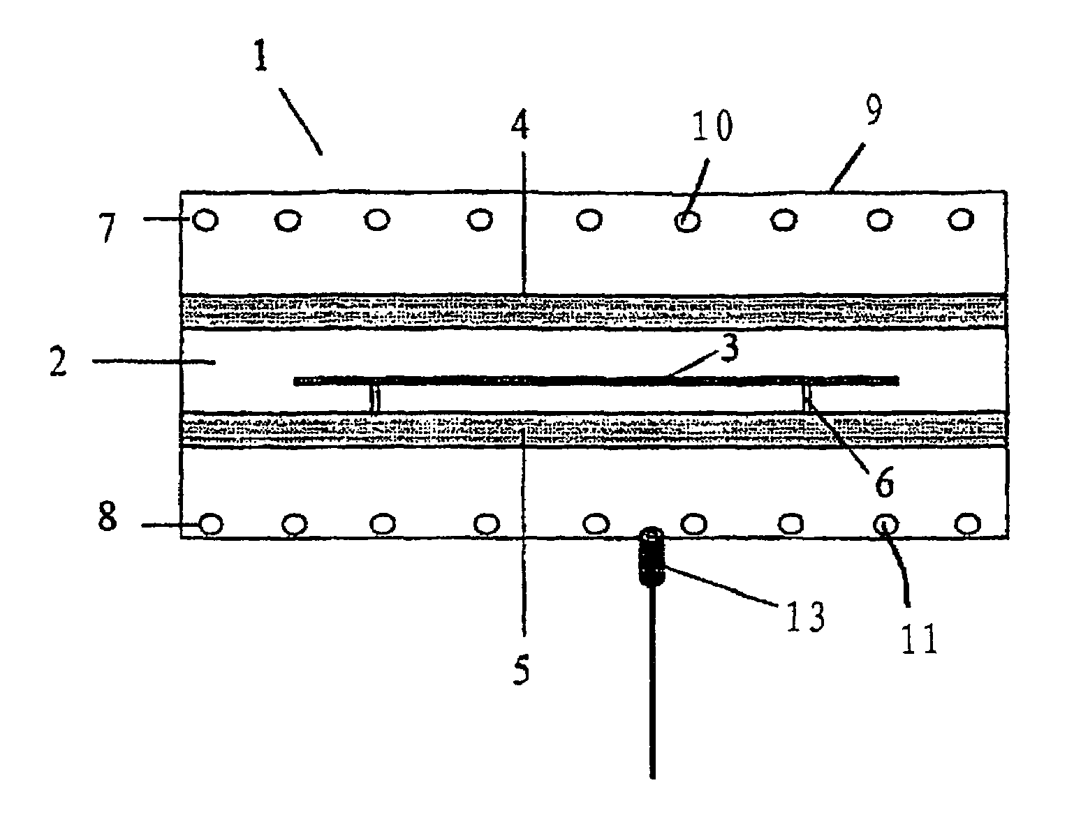
[0034]FIG. 1 shows, in cross-section, a rapid heating system 1 for the rapid heating of semiconductor wafers pursuant to a first embodiment of the invention. A process chamber 2, which accommodates a semiconductor wafer 3, is formed by an upper transparent plate 4 and a lower transparent plate 5, preferably quartz plates. In the process chamber 2, the wafer 3 that is to be processed is placed upon a support device 6. Not indicated are inlets and outlets for process gases via which a gas atmosphere that is suitable for the process can be produced.

[0035]Mounted above and / or below the process chamber 2 are heating devices in the form of banks of lamps 7 and 8. The plates 4 and 5 are disposed between the wafer 3 and the banks of lamps 7 and 8, and thus have the effect of a transparent shield for the formation of a closed process chamber. The entire arrangem...


PUM

PropertyMeasurementUnit
Timeaaaaaaaaaa
Wavelengthaaaaaaaaaa

Abstract

The object of the invention is to measure temperature using pyrometers, in a simple and economic way, enabling precise temperature measurement, even for low temperatures. The invention presents a device and method for thermally treating substrates, wherein the substrate is exposed to at least a first and at least a second radiation; the predetermined wavelengths of the first radiation are absorbed between the first radiation source and the substrate; a radiation from the substrate is measured in the predetermined wavelength using a radiation detector arranged on the same side as a second radiation source; the second radiation from the second radiation source is modulated and determined.

Description

BACKGROUND OF THE INVENTION[0001]The present invention relates to a method and to an apparatus for the thermal treatment of substrates, especially semiconductor wafers.[0002]Computer chips, as well as other electronic components, are produced on semiconductor disks, so-called wafers, which are subjected to thermal processes during the manufacturing sequence. These thermal processes require a defined temperature profile of the wafer at a defined atmosphere, in vacuum or defined underpressure or over pressure.[0003]For the temperature treatment of wafers, rapid heating units, also known as RTP units (Rapid Thermal Processing units), are being emphasized more and more. With these units a rapid and well-defined thermal treatment of wafers under prescribed process conditions is possible. RTP units permit a heating of the wafer that is to be treated, as a function of the wafer material, up to 1700° C. and more within a few seconds. A controlled or regulated heating up of the wafer pursuan...

Claims


Application Information

Patent Timeline
IPC IPC(8): C23C16/00G01J1/00H01L21/31C23C16/48C30B31/12C30B33/02H01L21/00H01L21/26H05B3/00
CPCC23C16/481C30B31/12C30B33/02H01L21/67248H05B3/0047H01L21/67115Y10T29/41H01L21/67242H01L21/324
Inventor HAUF, MARKUSSTRIEBEL, CHRISTOPH
Owner BEIJING E TOWN SEMICON TECH CO LTD
Why Eureka
Try Eureka