MEMS device made of transition metal-dielectric oxide materials

a technology of transition metal and dielectric oxide, which is applied in the direction of microstructural devices, microstructure devices, radiofrequency control devices, etc., can solve the problems of mems materials that also undergo oxidation when exposed to oxygen, mems materials that are also susceptible to oxidation, etc., and achieve suitable hardness and elasticity characteristics. , the effect of reducing the risk of oxidation

Inactive Publication Date: 2006-06-06
TEXAS INSTR INC +1
View PDF38 Cites 37 Cited by
  • Summary
  • Abstract
  • Description
  • Claims
  • Application Information

AI Technical Summary

Benefits of technology

[0018]Oxide-based materials for MEMS applications can have desirable stress, hardness, elasticity and other properties for use as structural material in a MEMS device. Unfortunately, many oxide materials, such as oxides of aluminum or silicon are insulating materials. This can be a problem with contacting surfaces in MEMS due to a lack of charge dissipation in insulators. Because of the lack of charge dissipation, use of insulators in MEMS can be problematic. Also, MEMS materials can also undergo oxidation when exposed to oxygen when used or fabricated, especially at high temperatures. Other problems with MEMS materials also exist. In the present invention, MEMS materials are utilized that are preferably conductive, resistant to oxidation and/or have suitable hardness and elasticity characteristics. In the present invention, MEMS devices (micro electromechanical systems, micro optoelectromechanical systems, micromechanical systems, etc.) are provided that are capable of movement due to a flexible portion formed of a (preferably conductive) oxide material, the material comprising a plurality of a transition metal and a selected element from group 3A or 4A or the periodic table, namely boron, aluminum, indium, silicon, germanium, or tin, and oxygen. Though preferred, the oxide material of the present invention need not be conductive nor resistant to oxidation. Also, though preferred, the flexible portion of the MEMS device need not be formed of the oxide material, but instead, a structural portion that does not bend or flex could comprise the oxide material. In one embodiment of the invention, both stiff structural portions as well as plasticizing portions comprise the oxide material.
[0019]The oxide film in the inventio

Problems solved by technology

Unfortunately, many oxide materials, such as oxides of aluminum or silicon are insulating materials.
This can be a problem with contacting surfaces in MEMS due to a lack of charge dissipation in insulators.
Because of the lack of charg

Method used


Image

  • MEMS device made of transition metal-dielectric oxide materials
  • MEMS device made of transition metal-dielectric oxide materials
  • MEMS device made of transition metal-dielectric oxide materials

Examples


Embodiment Construction

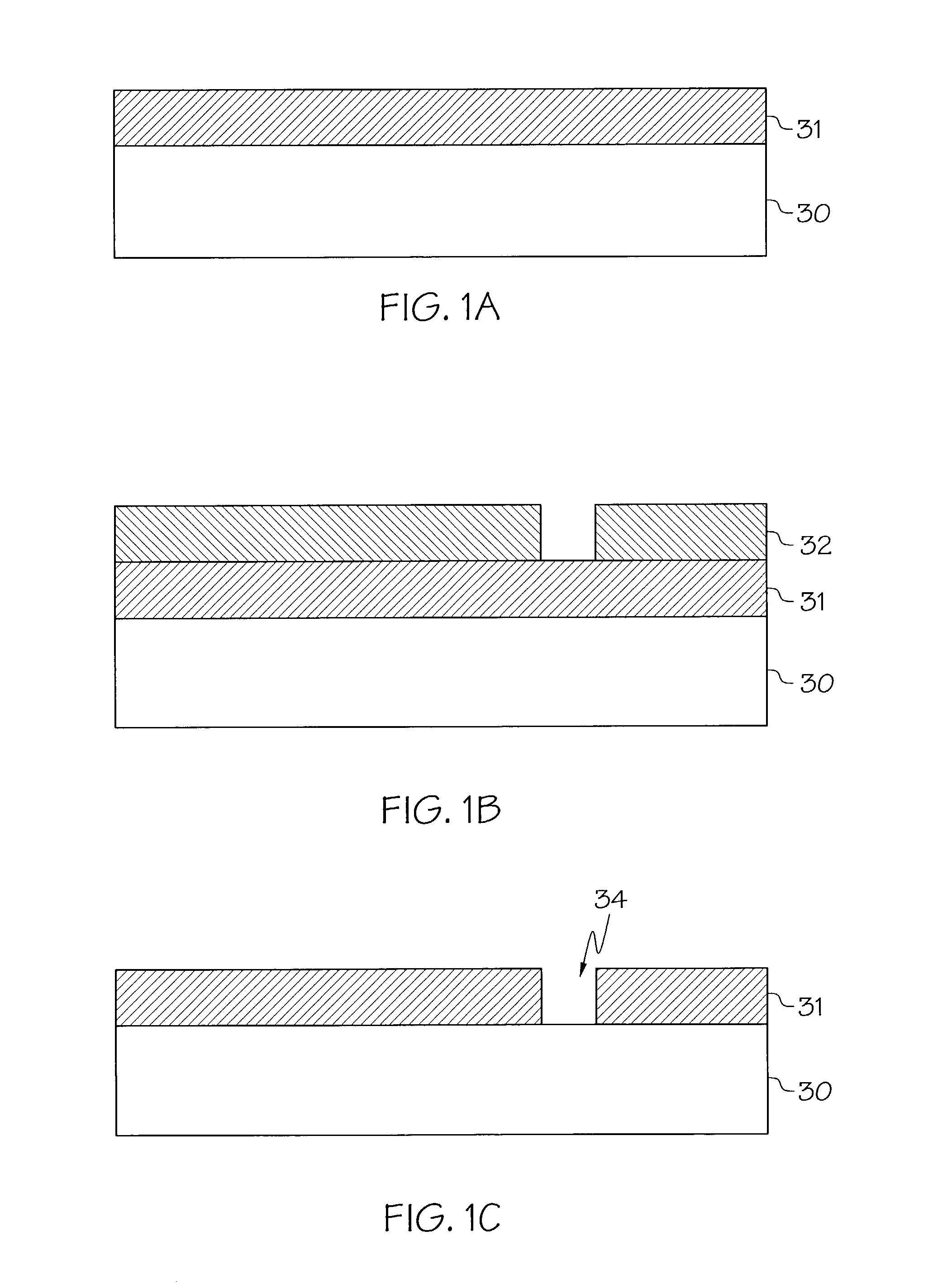
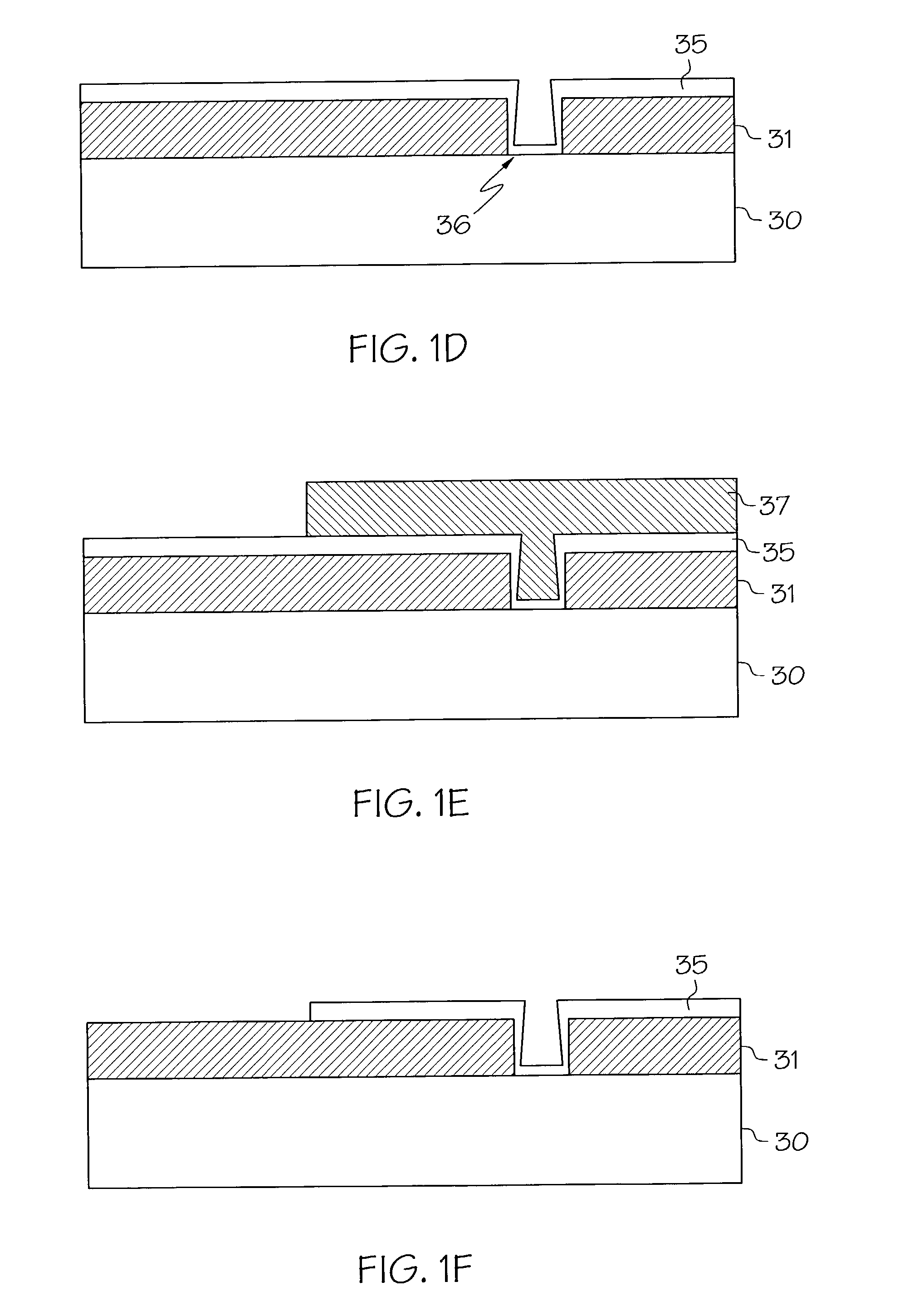
Micromechanical Structure Fabrication:

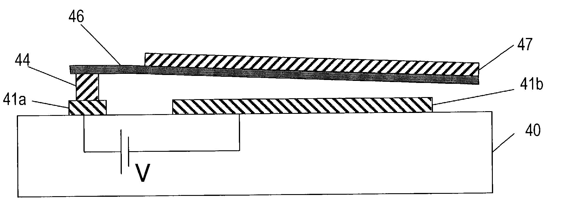
[0024]Some of the materials of the present invention are known, such as for high temperature oxidation resistant barriers. However, as will be discussed below, such materials have not been used for MEMS devices, such as for hinges or other flexible portions of MEMS devices. A wide variety of MEMS devices can be made in accordance with the present invention, including sensors (e.g. pressure sensors and accelerometers); movable elements in microfluidics such as microvalves, micropumps and micronozzles; micromirrors for optical scanning, microscopy, spectroscopy, maskless lithography, projection displays and optical switching; MEMS switches such as DC relays and RF MEMS switches; variable capacitors, variable inductors and variable optical attenuators; phased array antennas and other military MEMS applications, microfabricated resonators, gyroscopes, microturbines, etc. The examples below are micromirrors, however any of these or other MEMS devices...


PUM

PropertyMeasurementUnit
Currentaaaaaaaaaa
Currentaaaaaaaaaa
Currentaaaaaaaaaa

Abstract

Micromechanical devices are provided that are capable of movement due to a flexible portion. The micromechanical device can have a flexible portion formed of an oxide of preferably an element from groups 3A to 6A of the periodic table (preferably from the first two rows of these groups) and a late transition metal (preferably from groups 8B or 1B of the periodic table). The micromechanical devices can be any device, particularly MEMS sensors or actuators preferably having a flexible portion such as an accelerometer, DC relay or RF switch, optical cross connect or optical switch, or a micromirror part of an array for direct view and projection displays. The flexible portion is preferably formed by sputtering a target having a group 8B or 1B element and a selected group 3A to 6A element, namely B, Al, In, Si, Ge, Sn, or Pb. The target can have other major constituents or impurities (e.g. additional group 3A to 6A element(s)). The target is reactively sputtered in a oxygen ambient so as to result in a sputtered hinge. It is possible to form both stiff and/or flexible portions of the micromechanical device in this way.

Description

[0001]This application is a continuation-in-part of U.S. patent application Ser. No. 09 / 910,537 filed Jul. 20, 2001, the subject matter being incorporated herein by reference.BACKGROUND[0002]1. Field of Invention[0003]The following publications are related to the present invention:[0004]1) K. Onisawa, M. Fuyama, and K. Tamura, “Dielectric Properties of rf-Sputtered Y2O3 Thin Films,” J. Appl. Phys. 68, 719 (1990);[0005]2) 145. C. T. Hsu, Y. K. Su, and M. Yokoyama, “High Dielectric Constant of RF-Sputtered HfO2 Thin Films,” Jpn. J. Appl. Phys. 31, 2501 (1992);[0006]3) R. M. BUENO, J. M. MARTINEZ-DUART, M. HERNÁNDEZ-VÉLEZ, L. VÁZQUEZ “Optical and structural characterization of R.F. sputtered CeO2 thin films” J. Mat. Sci.,32, (1997), 1861–1865;[0007]4) A. K. Chu, M. J. Chuang, K. Y. Hsieh, H. L. Huang, Y. C. Yu, C. W. Wang, and E. K. Lin “Microstructure and Corrosion Resistance of Room-Temperature RF Sputtered Ta2O5 Thin Films”, J. Electr. Mat. (1999) 1457–1460;[0008]5) W. A. Bearzotti,...

Claims


Application Information

Patent Timeline
IPC IPC(8): H01L31/0232B81B3/00
CPCB81B3/0078B81B2203/0118B81B2201/045
Inventor REID, JASON S.
Owner TEXAS INSTR INC
Why Eureka
Try Eureka