Standby current reduction over a process window with a trimmable well bias

a technology of standby current and process window, which is applied in the direction of power consumption reduction, pulse technique, instruments, etc., can solve the problems of high manufacturing cost, high manufacturing cost, and inability to meet the requirements of manufacturing operation, and achieve low cost, high density, and efficient manufacturing.

Inactive Publication Date: 2006-06-13
POLARIS INNOVATIONS LTD
View PDF5 Cites 20 Cited by
  • Summary
  • Abstract
  • Description
  • Claims
  • Application Information

AI Technical Summary

Benefits of technology

[0007]In one aspect, the present invention relates to an integrated circuit device formed with MOSFETs, including an adjustable voltage source on the integrated circuit device. The adjustable voltage source is configured to control an operating characteristic of the device by providing a voltage difference between a body or substrate contact of the integrate circuit and source terminals of the MOSFETs. Critical operating characteristics such as leakage current or switching speed that affect device performance, particularly for integrated circuits processed with fine line structures that may include short gate structures, depend substantially on processing variables. In response to the difficulty or impracticality to control such variables during manufacture to suitable levels of accuracy, particularly from lot to lot, the on-die voltage source is adjusted. The operating characteristic of interest is measured after die processing in a post-processing test, and an external voltage source is applied and adjusted to determine the voltage required to control the operating characteristic. Then the adjustable voltage source on the die is adjusted by clearing on-die fuses, for example, to match the voltage of the external voltage source. Alternatively, resistive paths may be trimmed on the die using techniques such as laser vaporization to provide the required adjusted voltage. Thereby the design and efficient manufacture of high density and low cost integrated circuit devices is enabled.
[0012]Another embodiment of the present invention is a method of configuring an integrated circuit device formed with MOSFETs, and including an adjustable voltage source on the integrated circuit device. The method includes configuring the adjustable voltage source to control an operating characteristic of the device by providing a voltage difference between a body or substrate contact of the integrate circuit and source terminals of the MOSFETs. Critical operating characteristics such as leakage current or switching speed that affect device performance, particularly for integrated circuits processed with fine line structures and including short gate structures, depend substantially on processing variables. In response to the difficulty or impracticality to control such variables during manufacture to suitable levels of accuracy, particularly from lot to lot, the method includes adjusting the on-die voltage source. The method further includes measuring an operating characteristic of interest after processing the die in a post-processing test, and applying an external voltage source and adjusting it to determine the voltage required to control the operating characteristic. The method further includes adjusting the voltage source on the die by clearing on-die fuses, for example, to match the voltage of the external voltage source. Alternatively, method includes trimming resistive paths on the die using techniques such as laser trimming to provide the required adjusted voltage. Thereby the method enables the design and efficient manufacture of high density and low cost integrated circuit devices.

Problems solved by technology

Variations in threshold voltage and switching speed in MOSFETs are caused by unavoidable variations in device parameters such as gate oxide thickness, variations in various material impurities even at very low concentrations normally achieved in the refined semiconductor materials, variations in substrate doping density, variations in dimensions of the very small structures used to form the transistors, and variations in device operating temperature.
However, to precisely control device parameters in manufacturing processes, and particularly to precisely control their variations against worst-case effects with sufficient precision to produce the necessary yield in a manufacturing operation is often impractical in the leading edge designs that utilize the smallest of feature sizes.
The necessary manufacturing precision often requires unusual time and effort, and is generally inconsistent with the need to produce integrated circuits in high volumes at very low cost.
Present alternatives are to make compromises in end product performance by widening design margins and to accept reductions in manufacturing yield, all of which ultimately contribute to increased costs or marketing issues.
A further alternative to adjust device parameters such as threshold voltage by including an additional ion implantation late in the manufacturing process is generally considered to be impractical.
A limitation of these prior art designs is their general inability after wafer and die processing to accurately compensate a die containing a plurality of MOSFET devices of a similar conductivity type and geometry by selecting and setting a body bias voltage for the general variation of characteristics resulting from observed manufacturing variations.

Method used


Image

  • Standby current reduction over a process window with a trimmable well bias
  • Standby current reduction over a process window with a trimmable well bias
  • Standby current reduction over a process window with a trimmable well bias

Examples


Embodiment Construction

[0023]The making and using of the presently preferred embodiments are discussed in detail below. It should be appreciated, however, that the present invention provides many applicable inventive concepts that can be embodied in a wide variety of specific contexts. The specific embodiments discussed are merely illustrative of specific ways to make and use the invention, and do not limit the scope of the invention.

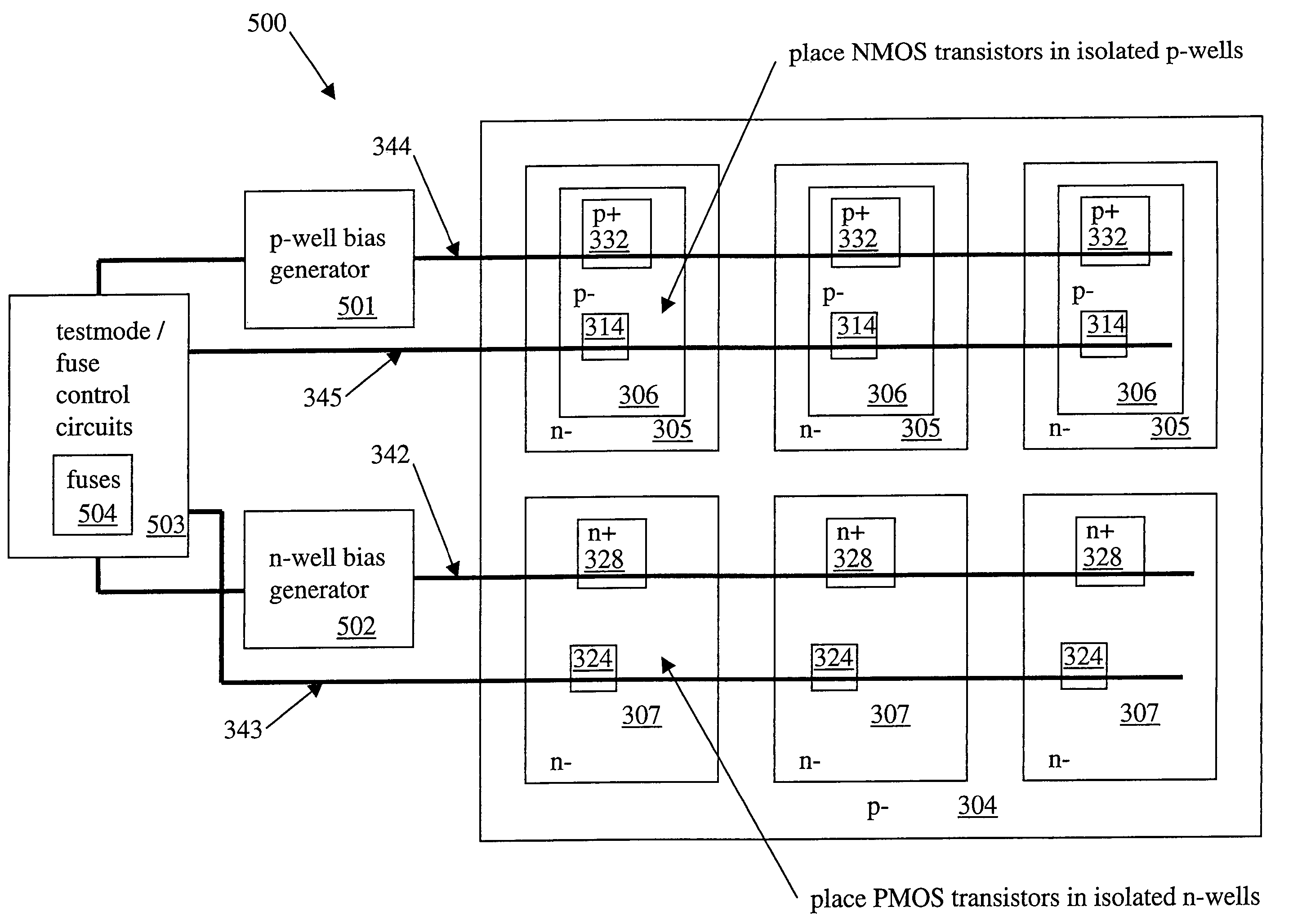
[0024]Embodiments of the present invention will be described with respect to preferred embodiments in a specific context, namely an integrated circuit including MOSFET devices configured with a trimmable well bias that is adjustable in a testmode process after die processing to improve an operating characteristic of a device, for example, to reduce standby current or to improve switching characteristics. The invention may be applied to logic or DRAM memory devices and other MOS integrated circuits to improve an operating characteristic over a design or manufacturing process w...


PUM


Abstract

An integrated circuit device including a plurality of MOSFETs of similar type and geometry is formed on a substrate with an ohmic contact, and an adjustable voltage source on the die utilizing clearable fuses is coupled between the ohmic contact and the sources of the MOSFETs. After die processing, a post-processing test is performed to measure an operating characteristic of the die such as leakage current or switching speed, and an external voltage source is applied and adjusted to control the operating characteristic. The on-die fuses are then cleared to adjust the on-die voltage source to match the externally applied voltage. The operating characteristic may be determined by including a test circuit on the die to exhibit the operating characteristic such as a ring oscillator frequency. This approach to controlling manufacturing-induced device performance variations is well suited to efficient manufacture of small feature-size circuits such as DRAMs.

Description

TECHNICAL FIELD[0001]Embodiments of the present invention relate generally to semiconductor circuits, and in particular to integrated circuits such as DRAMs. Included are any integrated circuits configured with metal-oxide semiconductor field-effect transistors (MOSFETs) in which the bodies of transistors are biased with a voltage to adjust an operating characteristic such as leakage current or switching speed.BACKGROUND[0002]Semiconductors are generally used in integrated circuits for a wide range of electronic applications, including radios, televisions, cell phones, and personal computing devices, as examples. Over the years of development of integrated circuit, the structures used to form the integrated circuit elements such as transistors and diodes have been continually reduced in size to enable production of ever more complex devices in small sizes, with improved performance, and with low cost. An example of a highly integrated semiconductor device is a dynamic random access ...

Claims


Application Information

Patent Timeline
Patent Type & Authority Patents(United States)
IPC IPC(8): H01L21/336H01L27/092H01L29/76H03K3/00H03K19/00
CPCH01L27/0925H03K19/0013H01L27/0928Y10S257/901
Inventor VOGELSANG, THOMAS
Owner POLARIS INNOVATIONS LTD
Why Eureka
Try Eureka