Field effect transistor

a field-effect transistor and transistor technology, applied in semiconductor devices, semiconductor/solid-state device details, electrical apparatuses, etc., can solve problems such as avalanche breakdown, and achieve the effects of miniaturizing gate length, increasing blocking voltage, and further miniaturizing gate length

Inactive Publication Date: 2006-06-27
RENESAS TECH CORP
View PDF11 Cites 13 Cited by
  • Summary
  • Abstract
  • Description
  • Claims
  • Application Information

AI Technical Summary

Benefits of technology

[0009]In the light of the state of the art described above, it is an object of the present invention to provide an improved structure of a MOS field effect transistor which can afford a high blocking voltage with a significantly miniaturized structure.
[0013]By contrast, in the MOS field effect transistor according to the present invention, the distance between the field relaxation layer and the high-density layer can be increased without being accompanied with enlargement in size of the device, whereby the blocking voltage can be increased, which in turn means that for a same blocking voltage, the gate length L can be realized minutely or shortened.
[0015]In the MOS field effect transistor according to the present invention, the high-density layers which are in contact with the source electrode and the drain electrode, respectively, are out of contact with the gate insulation film, which means nothing but the high-density layer is disposed with a given distance from the gate insulation film. By virtue of this feature, the distance between the field relaxation layer and the high-density layer can further be increased with the voltage directly applied to the gate insulation film can be relaxed or buffered.
[0017]In the MOS field effect transistor according to the present invention, the high-density layer is not placed in contact with the gate insulation film. Accordingly, there arises no necessity of increasing the thickness of the gate insulation film, differing from the conventional MOS field effect transistor, and thus the MOS field effect transistor according to the present invention can be protected against degradation of the performance. Thus, according to the present invention, there is realized the MOS field effect transistor which can afford the blocking voltage ranging from 5 to 15 volts and which can thus advantageously be incorporated in the flash memory.
[0018]In the MOS field effect transistor according to the present invention, an insulation film is deposited over the whole surface after having formed the gate electrode, whereon the high-density layers are deposited by using as a mask the side walls of the gate electrode formed by etch-back process such as anisotropical dry etching method. Consequently, there arises no problem concerning the distance between the field relaxation layer and the high-density layer while the high-density layers which are in contact with the source electrode and the drain electrode, respectively, can be disposed symmetrically relative to the gate electrode. Thus, a high blocking voltage can be assured without increasing the size of the device.
[0019]The teachings of the present invention can advantageously be applied to the implementation of the MOS field effect transistor whose blocking voltage lies in the range of about 5 to 15 volts. However, in order to realize the MOS field effect transistor whose blocking voltage ranges from 15 to 30 volts or so, the present invention further teaches that the field relaxation layer mentioned previously is made to extend from beneath the end face of the gate insulation film toward the source electrode for a distance of 0.15 μm or more. In that case, not only the distance between the field relaxation layer and the high-density layer is increased but also the field intensity can further be relaxed by the gate insulation layer. Thus, the blocking voltage or breakdown strength can be enhanced. Besides, the gate length can be shortened moreover.

Problems solved by technology

More specifically, when a voltage is applied to the drain electrode, a depletion layer ascribable to a PN junction formed between the field relaxation layer of the second conductivity type and the semiconductor substrate of the first conductivity type spreads to reach the high-density layer of the second conductivity type, as a result of which the field intensity at an end of the high-density layer increases, bringing about an avalanche breakdown.

Method used


Image

  • Field effect transistor
  • Field effect transistor
  • Field effect transistor

Examples


embodiment 1

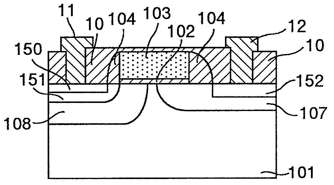
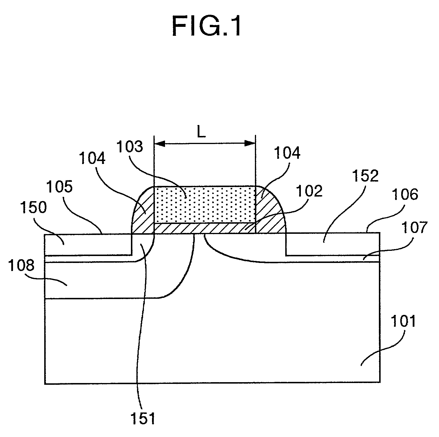
[0035]FIG. 1 is a sectional view showing-an N-type channel MOS (Metal Oxide Semiconductor) field effect transistor according to a first embodiment of the present invention. As can be seen in FIG. 1, the field effect transistor according to the instant embodiment of the present invention includes a P-type silicon substrate or a P-type well region 101 formed in either a P-type silicon substrate or an N-type silicon substrate by implanting P-type impurity ions such as boron ions, wherein formed on the P-type well region 101 are a gate silicon oxide film (gate insulation film) 102, a gate electrode 103 implemented in a laminated structure film composed of an N-type polysilicon layer doped with phosphorus and a tungsten silicide film, side walls 104 constituted by silicon oxide films formed on lateral surfaces, respectively, of the gate electrode 103, a source region 105 constituted by a high-density N-type layer (N+-layer) 150 formed in contact with either one of the side walls 104 and ...

embodiment 2

[0039]FIG. 3 is a sectional view showing an N-type channel MOS field effect transistor according to a second embodiment of the present invention. In the figure, like reference symbols as those used in FIG. 1 denote equivalent or corresponding parts. Referring to FIG. 3, the N-type channel MOS field effect transistor according to the instant embodiment of the invention includes, being formed in the P-type well region 101 similarly to the first embodiment of the invention, a gate silicon oxide film (gate insulation film) 102, a gate electrode 103, side walls 104 formed on lateral surfaces, respectively, of the gate electrode 103, a source region 105 constituted by a high-density N-type layer (N+-layer) 150 formed in contact with one of the side walls 104 mentioned above and a low-density N-type layer (N−-layer) 151 which is formed between the high-density N-type layer 150 and the gate insulation film 102 and which has a lower density than the high-density N-type layer 150, and a drain...

embodiment 3

[0043]FIG. 4 is a sectional view showing an N-type channel MOS field effect transistor according to a third embodiment of the present invention. In the figure, like reference symbols as those used in FIG. 1 denote equivalent or corresponding parts.

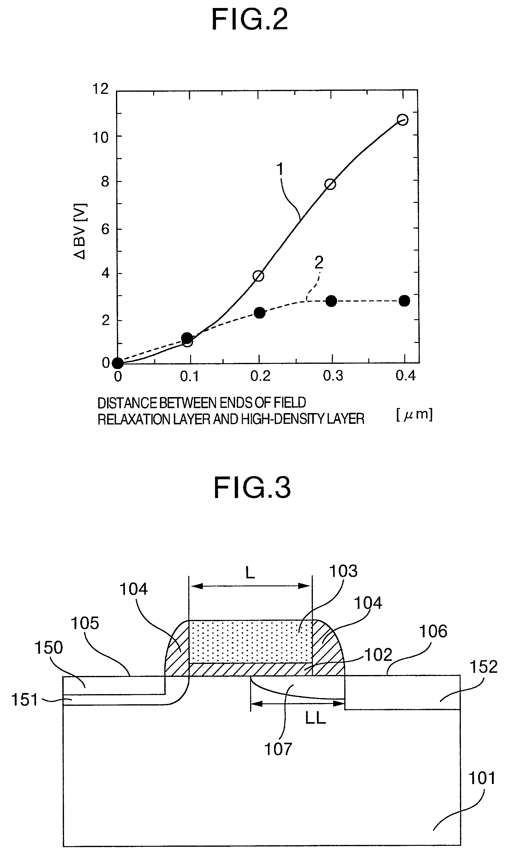
[0044]The N-type channel MOS field effect transistor according to the third embodiment of the invention differs from the first embodiment in that a P-type impurity layer 109 is additionally formed by doping boron or the like in and along the surface of the drain region 106 of the N-type channel MOS field effect transistor according to the first embodiment. In the case of the N-type channel MOS field effect transistor according to the first embodiment, the high-density N+-layer 152 is distanced from the gate insulation film 102 so that the voltage applied to the drain electrode is not directly applied to the gate insulation film 102. In this conjunction, it is noted that when the blocking voltage demanded for the device is to be set high, t...


PUM


Abstract

A MOS field effect transistor. A field relaxation layer of a gate overlap structure is disposed in contact with a drain region for the purpose of relaxation of the electric field by increasing a distance between the field relaxation layer and a high-density layer. The electric field relaxation can further be promoted because the equipotential lines are bent by a gate insulation film. A punch-through stopper layer of a gate overlap structure is disposed in contact with a source region for suppressing spreading of a depletion layer toward the source region. The length of a gate electrode can be realized in a miniaturized size.

Description

BACKGROUND OF THE INVENTION[0001]1. Field of the Invention[0002]The present invention relates to a MOS (Metal Oxide Semiconductor) field effect transistor whose blocking voltage appearing between a drain electrode and a substrate (between a drain electrode and a source electrode) is higher than 5 volts inclusive.[0003]2. Description of Related Art[0004]For implementing a flash memory or the like device which requires a voltage of about 10 volts or higher for memory cell write / erase operations, there are required MOS field effect transistors (MOSFETs) whose blocking voltage is on the order of 10 volts. In Japanese Patent Application Laid-Open Publication No. 8580 / 1995 (JP-A-7-8580), a MOS field effect transistor which exhibits a relatively high blocking voltage of about 30 volts and in which a high-density layer formed in contact with a drain electrode is disposed relative to a high-density layer formed in contact with the source electrode with interposition of an insulation film hav...

Claims


Application Information

Patent Timeline
Patent Type & Authority Patents(United States)
IPC IPC(8): H01L31/119H01L21/336H01L21/8234H01L21/8238H01L27/088H01L27/092H01L29/08H01L29/10H01L29/78
CPCH01L21/823412H01L27/088H01L29/7835H01L29/1083H01L29/66659H01L29/0847H01L21/18
Inventor OHYANAGI, TAKASUMIWATANABE, ATSUO
Owner RENESAS TECH CORP
Why Eureka
Try Eureka