

Catoptric projection optical system
a projection optical system and catoptric technology, applied in the field of reflection type or catoptric projection optical system, can solve the problems of difficult to meet the requirements of using, the projection optical system cannot include any lenses, and the conventional three or four mirrors have a difficulty in reducing wave front aberration, etc., to achieve excellent imaging performance, reduce the maximum effective diameter and the overall length of the optical system, and achieve excellent imaging performance.
- Summary
- Abstract
- Description
- Claims
- Application Information
AI Technical Summary
Benefits of technology
Problems solved by technology
Method used
Image

Examples
Embodiment Construction
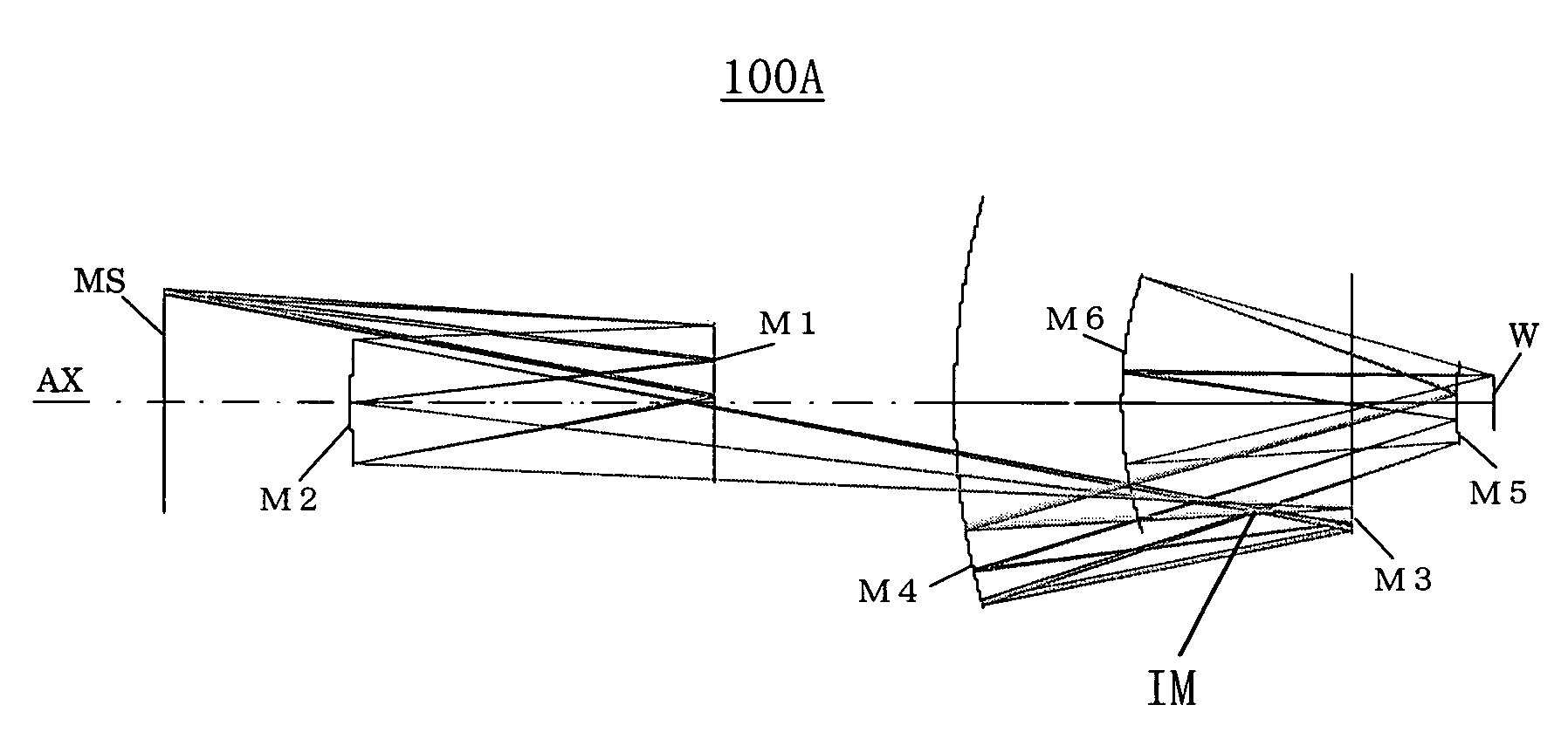
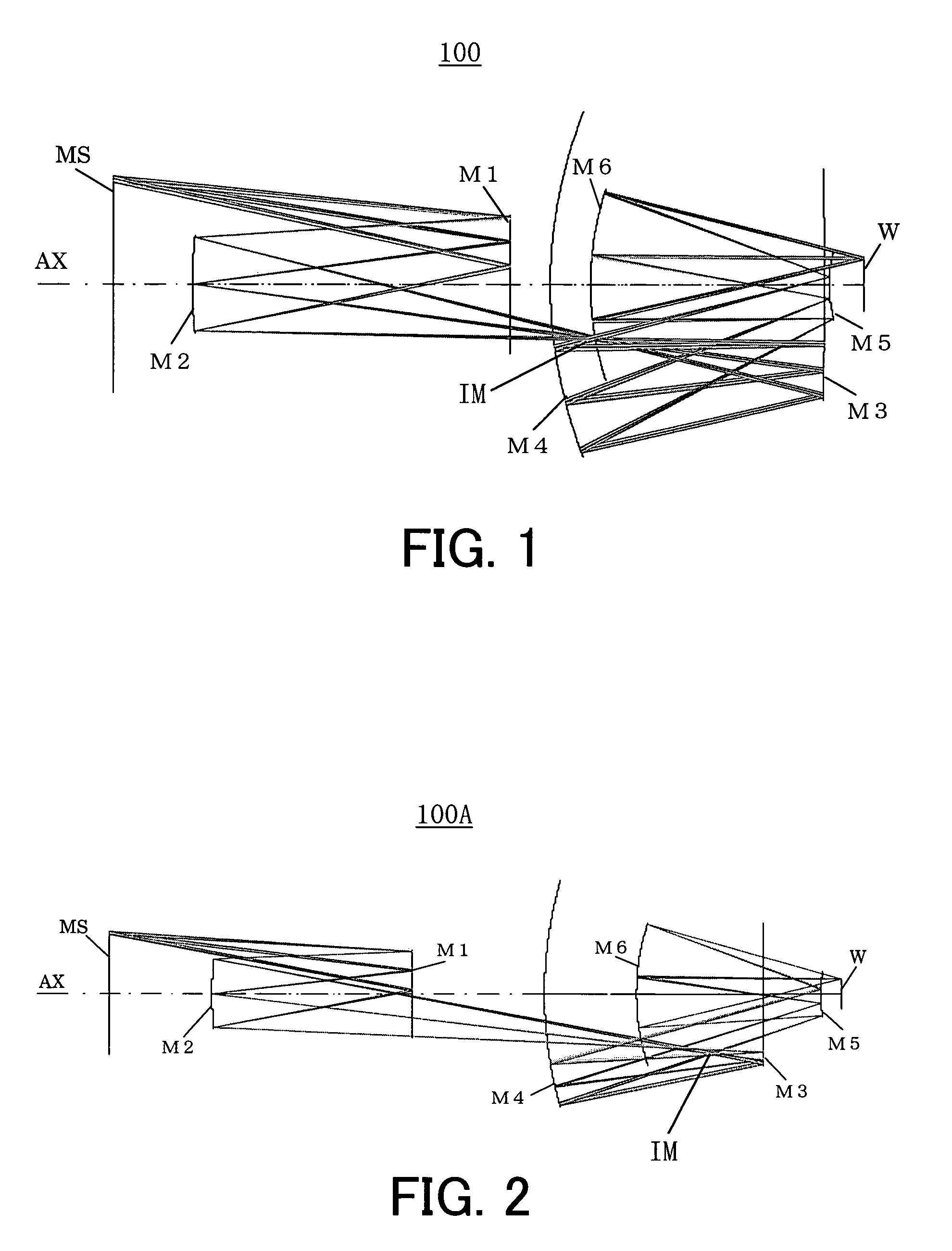
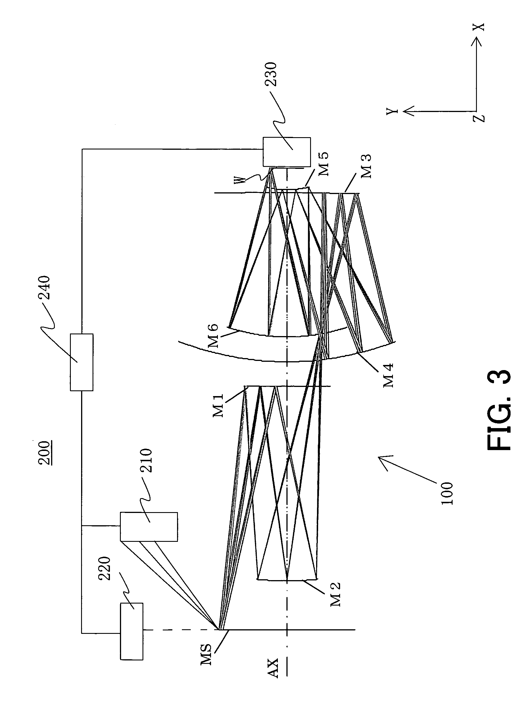
[0034]A description will now be given of catoptric projection optical systems 100 and 100A and an exposure apparatus 200 as one aspect of the present invention with reference to the accompanying drawings. The same reference numeral in each figure denotes the same element, and a description thereof will be omitted. Here, FIG. 1 is a schematic structure of the catoptric projection optical system 100. FIG. 2 is a schematic structure of the catoptric projection optical system 100A. Unless otherwise specified, the catoptric projection optical system 100 generalizes the catoptric reduction projection optical system 100A.
[0035]Referring to FIG. 1, the inventive catoptric projection optical system 100 reduces and projects a pattern on an object surface (MS), such as a mask surface, onto an image surface (W), such as a substrate surface and an object surface to be exposed. The catoptric projection optical system 100 is an optical system particularly suitable for the EUV light (with a wavelen...
PUM
| Property | Measurement | Unit |
|---|---|---|
| size | aaaaa | aaaaa |
| wavelength | aaaaa | aaaaa |
| wavelength | aaaaa | aaaaa |
Abstract
Description
Claims
Application Information