Method of fabricating polysilicon film by excimer laser crystallization process

Active Publication Date: 2006-07-04
CHINA STAR OPTOELECTRONICS INT HK
View PDF11 Cites 9 Cited by
  • Summary
  • Abstract
  • Description
  • Claims
  • Application Information

AI Technical Summary

Benefits of technology

[0011]It is an advantage of the claimed invention that the method not only forms a mask layer to control the location of grain boundary but also utilizes a heat-retaining capping layer to maintain the temperature of the amorphous

Problems solved by technology

However, the fully developed amorphous silicon thin film transistor liquid crystal display (a-Si TFT LCD) devices, which are restricted in their carrier transfer rate, have difficulty in meeting the requirements of being thin, being power saving, and having high resolution.
Thus, in a conventional method of fabricating a polysilicon thin film transistor, an expensive quartz substrate is needed and only a small size liquid crystal display panel ca

Method used


Image

  • Method of fabricating polysilicon film by excimer laser crystallization process
  • Method of fabricating polysilicon film by excimer laser crystallization process
  • Method of fabricating polysilicon film by excimer laser crystallization process

Examples


first embodiment

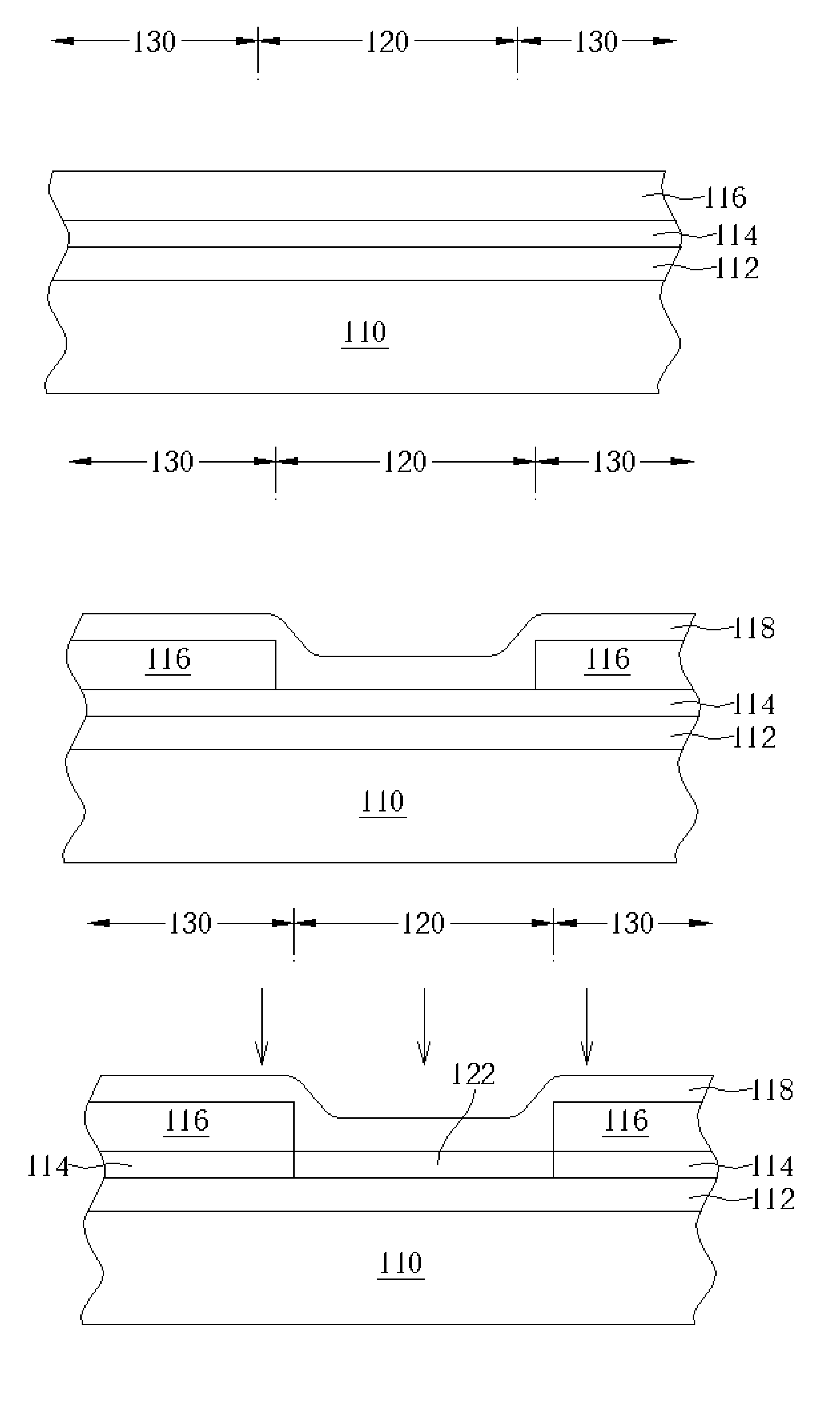
[0017]Please refer to FIG. 4 to FIG. 7, which are schematic diagrams of a method of fabricating a polysilicon film by an excimer laser crystallization process according to the present invention. As shown in FIG. 4, a substrate 110 is first provided. The substrate 110 is defined with a first region 120 and a second region 130. Then, a buffer layer 112 is formed on the substrate 110 to prevent the impure materials from diffusing upward in latter processes and affecting the quality of the polysilicon film. After that, an amorphous silicon film 114 is formed on the buffer layer 112 and a mask layer 116 is formed on the amorphous silicon film 114. In the preferred embodiment of the present invention, the substrate 110 is a glass substrate. The buffer layer 112 is a silicon oxide layer or a multi-layer structure composed of a silicon oxide layer and a silicon nitride layer. The mask layer 116 is a single layer structure composed of a silicon oxide layer, a silicon nitride layer, a metal l...

second embodiment

[0023]Generally speaking, the present invention utilizes a heat-retaining capping layer to reduce the heat dissipation after the excimer laser irradiation is stopped. Thus, the grains can be grown in an environment with a relative high temperature, leading to increase the grain size. With the assistance of the long pulse duration laser, the present invention can increase the grain size to about 10 μm, which improves the quality of the latter formed low temperature polysilicon thin film transistors. In addition, in the case of forming the heat-retaining capping layer before the mask layer, which is disclosed in the present invention, since the mask layer does not contact with the amorphous silicon film or the polysilicon film directly, no pollution is concerned while the mask layer is mainly composed of a metal layer.

[0024]In contrast with the prior art method, the present invention can not only control the location of the grain boundary, but also improve the grain size in the polysi...


PUM


Abstract

A method of fabricating a polysilicon film by an excimer laser crystallization process. First, a substrate comprising a first region and a second region is provided. An amorphous silicon layer and a mask layer are formed on the substrate in sequence. Then, a photo-etching process is performed to remove the mask layer in the first region. A heat-retaining capping layer is formed on the mask layer and the amorphous silicon layer. After that, an excimer laser crystallization process is performed so that the amorphous silicon layer in the first region is crystallized into a polysilicon film.

Description

BACKGROUND OF INVENTION[0001]1. Field of the Invention[0002]The present invention relates to a method of fabricating a polysilicon film, and more particularly, to a method of fabricating a polysilicon film by an excimer laser crystallization(ELC) process.[0003]2. Description of the Prior Art[0004]The progress of science and technology has led to small, effective, and portable intelligent information products becoming a part of our lives. Display devices play an important role because all intelligent information products, such as mobile phones, personal digital assistants (PDAs), or notebooks, need display devices to be a communication interface. However, the fully developed amorphous silicon thin film transistor liquid crystal display (a-Si TFT LCD) devices, which are restricted in their carrier transfer rate, have difficulty in meeting the requirements of being thin, being power saving, and having high resolution. Therefore, the a-Si TFT LCD devices are gradually replaced by low te...

Claims


Application Information

Patent Timeline
IPC IPC(8): H01L21/36H01L21/20H01L21/00
CPCH01L21/2026H01L21/02686H01L21/02422H01L21/02678H01L21/02502H01L21/02488H01L21/02532H01L21/02595
Inventor LIN, KUN-CHIH
Owner CHINA STAR OPTOELECTRONICS INT HK
Why Eureka
Try Eureka