Method for the dynamically balancing series- and parallel-wired power semiconductor circuits

a technology of power semiconductors and series- and parallel-wired circuits, applied in the field of power electronics, can solve the problems of uncontrolled time deviation in signal transmission, inability to carry out corrections, and comparatively undetermined relation between control loop offsets and required time delays. achieve the effect of high switching speed

Inactive Publication Date: 2006-07-04
POWER INTEGRATIONS INC
View PDF8 Cites 6 Cited by
  • Summary
  • Abstract
  • Description
  • Claims
  • Application Information

AI Technical Summary

Benefits of technology

[0004]It is an object of the invention to provide an improved method for dynamically balancing semiconductor power switches where an exact synchronization of the individual semiconductor power switches and a high switching speed of the complete circuit can be achieved.
[0008]In a further embodiment, actual values are measured at two synchronous sampling times and the control loop offset is determined from their gradient and from a desired gradient value, and an amplitude of the switching signal for which the control loop offset corresponds to a too high or too low gradient is decreased or increased in the same or one of the next switching cycles. In particular, a first sampling time is chosen closer in time to a reference time of the synchronous event and a difference between the sampling times is approximated by a second sampling time. By means of the additional gradient control, the accuracy of the dynamic synchronicity of the switching behavior of the semiconductor power switches can be improved again.

Problems solved by technology

A problem in this method are uncontrolled time deviations in the signal transmissions from the central control to the local measuring systems.
A further problem consists in the fact that the relation between the control loop offsets and the required time delays is comparatively undetermined and, at best, known empirically, and corrections can only be carried out in the following switching cycles.
In addition, the method also requires an adaptation of the central sampling time within a limited time window.

Method used


Image

  • Method for the dynamically balancing series- and parallel-wired power semiconductor circuits
  • Method for the dynamically balancing series- and parallel-wired power semiconductor circuits
  • Method for the dynamically balancing series- and parallel-wired power semiconductor circuits

Examples


Embodiment Construction

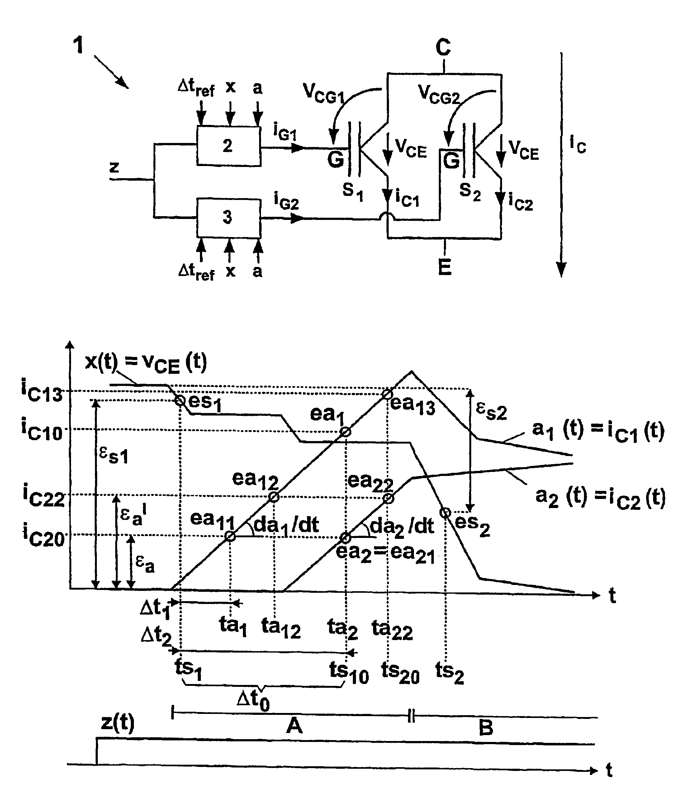
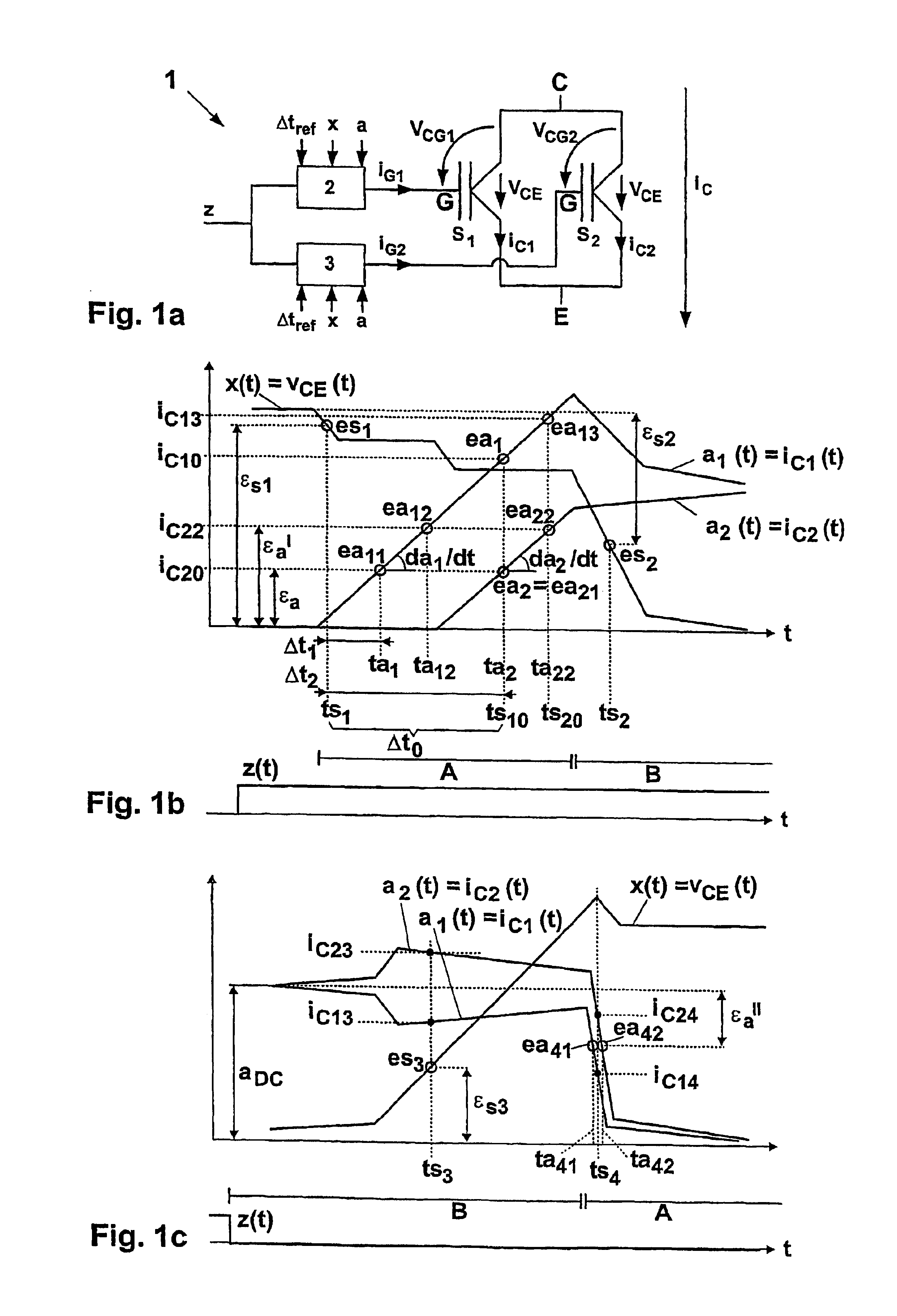
[0020]In FIG. 1a, each one of two parallel semiconductor power switches S1 and S2 is driven by a dedicated gate driver 2, 3, Each gate driver 2, 3 receives a central switching command z as well as, in addition, a desired time interval value Δtref as well as actual values and desired values of at least one synchronous event or a synchronous variable x and of at least one asynchronous variable a. Typically, the actual values x and a are measured locally at the semiconductor power switch S1 or S2. In gate driver 2, 3 a control signal or switching signal, namely a gate current iG1, iG2 or a gate voltage vCG1, vCG2 or a time integral of the gate current iG1, iG2 is generated based on the input values z, Δtref, x and a, and fed to the control terminal or the gate G of the semiconductor power switch S1 or S2. The collector-emitter voltage vCE (where applicable also called the anode-cathode voltage) is identical over the two semiconductor power switches S1 and S2 in the parallel circuit 1 a...


PUM


Abstract

A method for dynamically balancing the loads in a circuit (1, 4) of semiconductor power switches arranged in series or in parallel is disclosed. Individual switching signals (iG1, iG2) for the semiconductor power switches (S1 . . . S4) are generated by determining a system-widely valid synchronous sampling time (tsj) independently for each semiconductor power switch (S1 . . . S4) due to a synchronous event (es) of the whole circuit (1, 4). Control loop offsets between actual values (ai) measured synchronously at the sampling time (tsj) and given desired values (as) of an asynchronous state variable (a(t)) of the semiconductor power switches (S1 . . . S4) are reduced in the same or in following switching cycles. Alternatively, control loop offsets between actual time values (tai) and desired time values (tas) are minimized, wherein the actual time values (tai) are measured upon exceeding a globally provided threshold value (εa) of an asynchronous state variable (a(t)) of the semiconductor power switches (S1 . . . S4). Embodiments relate to: Offsetting the sampling time (tsj) in time by a globally provided time interval (Δt0), providing desired values locally or globally, e.g. by averaging of actual values (ai, tai), additional balancing of the gradients of asynchronous time variables (a(t)). A central sampling command can be dispensed with and the switching synchronicity is improved, switching times are shortened and dynamic switching losses are reduced.

Description

[0001]This application is a 371 national phase application of PCT / IB00 / 01968 filed on 27 Dec. 2000, the content of which is incorporated herein by reference in its entirety.TECHNICAL FIELD[0002]The invention lies in the field of power electronics. It relates to a method for dynamically balancing power semiconductor switches according to the preamble of the independent claims.STATE OF THE ART[0003]Such a method for dynamically synchronizing power semiconductor switches in series has been disclosed in the article of C. Gerster, “Fast High-power / High-voltage Switch Using Series-connected IGBTs with Active Gate-controlled Voltage-balancing”, Proceedings of 1994 Applied Power Electronics Conference and Exposition, Vol. 1, pp. 469-472, IEEE, New York (1994). A sampling time that is valid system-wide is provided by a central control. At this sampling time, the individual collector-emitter voltages of the IGBTs are determined by means of local measuring systems and individual difference vol...

Claims


Application Information

Patent Timeline
Patent Type & Authority Patents(United States)
IPC IPC(8): G05F1/40H03K17/30H03K17/10H03K17/12H03K17/687
CPCH03K17/10H03K17/127H03K17/12H03K17/107
Inventor THALHEIM, JAN
Owner POWER INTEGRATIONS INC
Why Eureka
Try Eureka