Image display unit and production method therefor

a technology of image display and production method, which is applied in the field of image display unit, can solve the problems of damage to the electron source, inability to display high-bright images, and disturbance of electron sources, and achieve high precision, high fineness, and high precision

Inactive Publication Date: 2006-07-11
KK TOSHIBA
View PDF8 Cites 9 Cited by
  • Summary
  • Abstract
  • Description
  • Claims
  • Application Information

AI Technical Summary

Benefits of technology

[0019]And, because the getter film having the pattern is formed as described above, the occurrence of electric discharge is restricted and the peak value of a discharge current is suppressed if electric discharge occurs in especially a flat type image display unit such as the FED, so that the electron emitting elements or the phosphor screen is prevented from being destructed, damaged or deteriorated.
[0020]In the method for manufacturing an image display unit of the present invention, when a method of vapor-depositing the getter material from the above of the pattern of the heat-resisting fine particle layer after the heat-resisting fine particle layer is formed in a specified pattern is adopted, the getter material-deposited film is formed on areas, where the heat-resisting fine particle layer is not formed, of the metal back layer, and the getter film having the pattern of the heat-resisting fine particle layer and the inversion pattern can be formed. And, by forming the getter film having the pattern as described above, especially the flat type image display unit such as the FED can restrict the occurrence of electric discharge and suppress the peak value of discharge current if electric discharge occurs, and the electron emitting elements or the phosphor screen can be prevented from being destructed, damaged or deteriorated.
[0021]And, the pattern of the heat-resisting fine particle layer can be formed in high fineness and high precision by a screen printing method or the like, so that the getter film in its reverse pattern can also be formed in high fineness and high precision.

Problems solved by technology

When gas (surface adsorption gas) adsorbed to the inner surface of the vacuum envelope is separated to lower a degree of vacuum in the envelope, electrons emitted from the electron source are disturbed from reaching the phosphor material, and a high-brightness image display cannot be made.
The gas generated in the envelope is ionized by the electron beam and accelerated by an electric field to collide the electron source, possibly damaging the electron source.
Therefore, when the surface adsorption gas in a volume similar to that of the CRT is released, deterioration of the degree of vacuum in the vacuum envelope becomes quite substantial.
The conventional field emission display (FED) had a disadvantage that an electric discharge (vacuum arc discharge) was easily caused when images were formed for a long period because a face plate having a phosphor screen and a rear plate having an electron emitting element had a very small gap (space) of one to several millimeters between them, and a high voltage of about 10 kV was applied to the small gap to form a high electric field.
And, when such an abnormal electric discharge occurred, a large discharge current in a range of several amperes to several hundred amperes flowed instantaneously, so that there was a possibility that the electron emitting element of a cathode section and the phosphor screen of an anode section were destructed or damaged.
But, this method has disadvantages that patterning accuracy, pattern fineness and the like are limited, and an advantageous effect of preventing an electric discharge to improve the withstand pressure characteristic is not sufficient.

Method used


Image

  • Image display unit and production method therefor
  • Image display unit and production method therefor
  • Image display unit and production method therefor

Examples


example 1

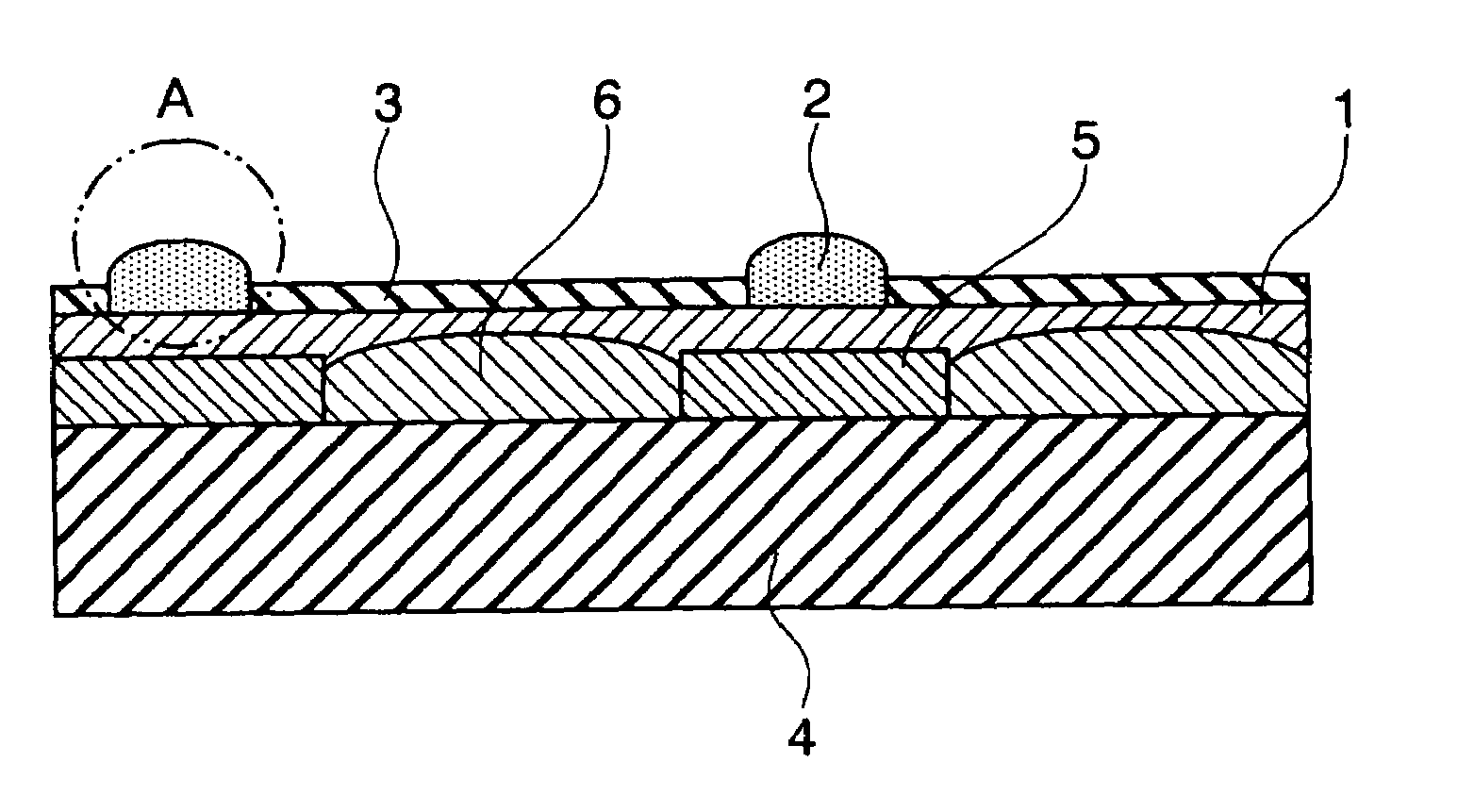
[0042]A light absorption layer (light-shielding layer) consisting of a black pigment was formed in a stripe form on a glass substrate by a photolithography, and a three color phosphor layer of red (R), green (G) and blue (B) was formed to have stripe patterns between the adjacent patterns of the light absorption layer by the photolithography. Thus, a phosphor screen having the light absorption layer and the phosphor layer with the specified patterns was formed.

[0043]Then, an Al film was formed as a metal back layer on the phosphor screen. Specifically, an organic resin solution mainly containing an acryl resin was applied to and dried on the phosphor screen to form an organic resin layer, an Al resin was formed thereon by vacuum-depositing, and heating was performed for baking at a temperature of 450° C. for 30 minutes so as to decompose and remove an organic component.

[0044]Next, a silica paste consisting of 5 wt % of silica (SiO2) fine particles (particle size of 10 nm), 4.75 wt %...

example 2

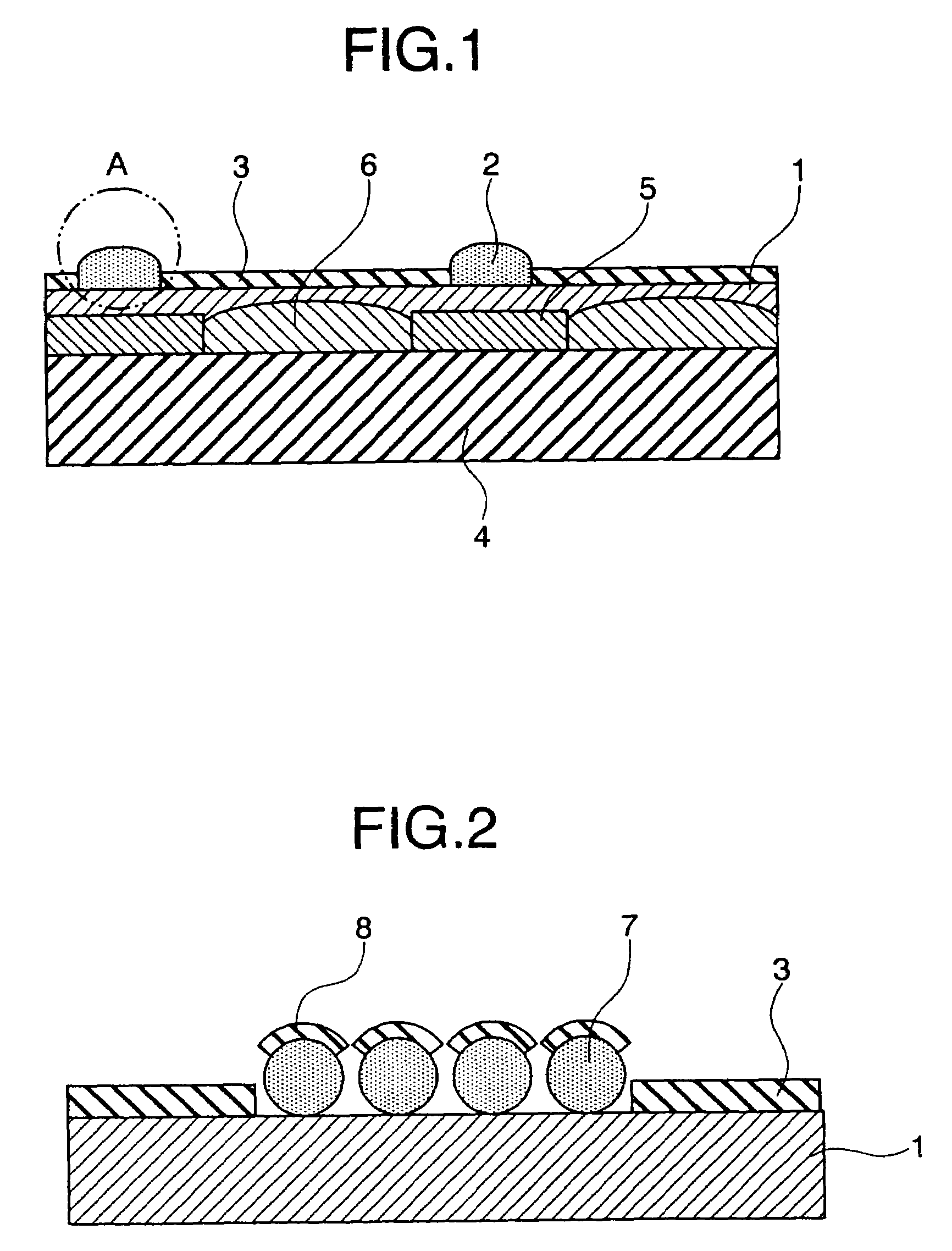
[0050]An Al film was formed on a phosphor screen formed in the same way as in Example 1, and a paste consisting of 10 wt % of Al2O3 fine particles having a particle size of 7 μm, 4.75 wt % of ethyl cellulose and 85.25 wt % of butyl carbitol acetate was screen-printed on the Al film to form a pattern of the Al2O3 layer.

[0051]Then, Ba was deposited on the formed pattern of the Al2O3 layer in the same way as in Example 1 to form a getter film (Ba film) having a reverse pattern of the pattern of the Al2O3 layer. Surface resistivity of the getter film was measured in a state that a vacuum atmosphere was retained. The measured result is shown in Table 1.

[0052]Using a panel having the patterned Al2O3 layer, on which the getter film was not deposited, as the face plate, an FED was produced in the same way as in Example 1. The withstand voltage characteristic of the obtained FED was determined for evaluation by a common procedure. And, fineness of the getter film pattern and a degree of elec...


PUM


Abstract

An image display unit having a structure in which a heat-resisting fine particle layer is formed on a metal back layer disposed on a phosphor layer, and a getter layer is deposited / formed on the heat-resisting fine particle layer by vapor-depositing. The fine particle layer is desirably formed in a specified pattern, and a filmy getter layer is formed in a pattern complementary to the former pattern. The average particle size of heat-resisting fine particles which may use SiO2, TiO2, Al2O3, Fe2O3 is 5 nm to 30 μm. Since abnormal discharging is restricted, the destruction and deterioration of an electron emitting element and a phosphor screen are prevented to provide a high-brightness, high-grade display.

Description

TECHNICAL FIELD[0001]The present invention relates to an image display unit and a method for manufacturing an image display unit. More specifically, the invention relates to an image display unit having an electron source and a phosphor screen forming an image by irradiation of an electron beam emitted from the electron source within a vacuum envelope and a manufacturing method thereof.BACKGROUND ART[0002]An image display unit, which displays an image by irradiating an electron beam which is emitted from an electron source to a phosphor material to cause the phosphor material to emit light, generally has the electron source and the phosphor material within a vacuum envelope. When gas (surface adsorption gas) adsorbed to the inner surface of the vacuum envelope is separated to lower a degree of vacuum in the envelope, electrons emitted from the electron source are disturbed from reaching the phosphor material, and a high-brightness image display cannot be made. Therefore, it is neces...

Claims


Application Information

Patent Timeline
Patent Type & Authority Patents(United States)
IPC IPC(8): H01J29/94H01J29/28H01J31/12H01J9/22H01J9/20H01J9/227H01J9/39H01J29/08H01J29/32
CPCH01J9/20H01J29/94H01J29/28H01J29/085H01J31/12
Inventor ITO, TAKEOOYAIZU, TSUYOSHINISHIMURA, TAKASHIKOIDE, SATOSHITABATA, HITOSHI
Owner KK TOSHIBA
Why Eureka
Try Eureka