Manufacturing method of semiconducter device

a manufacturing method and semiconductor technology, applied in the direction of transistors, solid-state devices, capacitors, etc., can solve the problems of deterioration of ferroelectric films, comparatively high voltage, and sharp deterioration of ferroelectric capacitor operating characteristics, so as to achieve favorable fatigue characteristics and increase the quantity of switching electric charges

Inactive Publication Date: 2006-07-18
FUJITSU SEMICON LTD
View PDF4 Cites 24 Cited by
  • Summary
  • Abstract
  • Description
  • Claims
  • Application Information

AI Technical Summary

Problems solved by technology

A tunnel current that passes through the insulating film has to be passed to write and erase the information, and thus comparatively high voltage is needed.
When the ferroelectric film is reduced, the operating characteristics of the ferroelectric capacitor are sharply deteriorated.
However, when such a conductive oxide film of the non-stoichiometric composition is exposed to an atmosphere including hydrogen, a metal component in the film activates hydrogen, and the activated hydrogen deteriorates the ferroelectric film.
It is possible that these foreign matters interfere with subsequent process steps, and therefore it is necessary to prevent the foreign matters from being formed.
However, even with adoption of any method of them, a sufficient quantity of switching electric charge to be demanded hereinafter cannot be obtained.

Method used


Image

  • Manufacturing method of semiconducter device
  • Manufacturing method of semiconducter device
  • Manufacturing method of semiconducter device

Examples


first embodiment

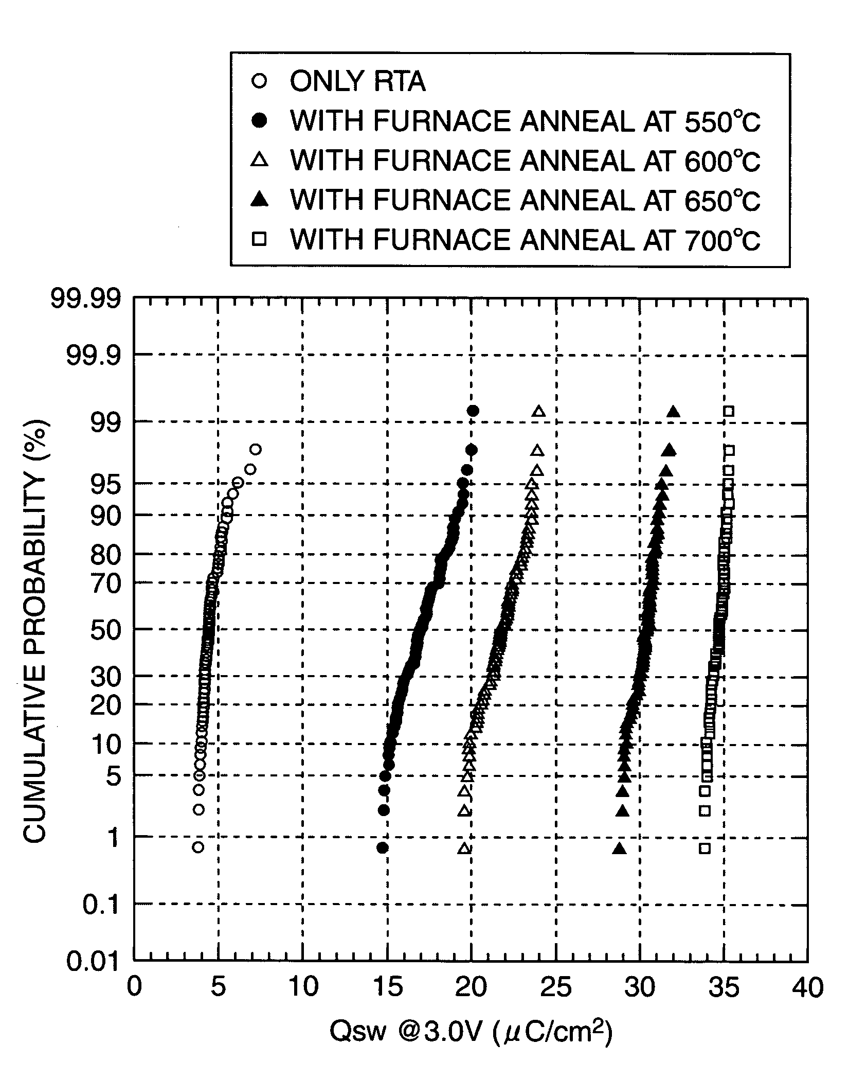
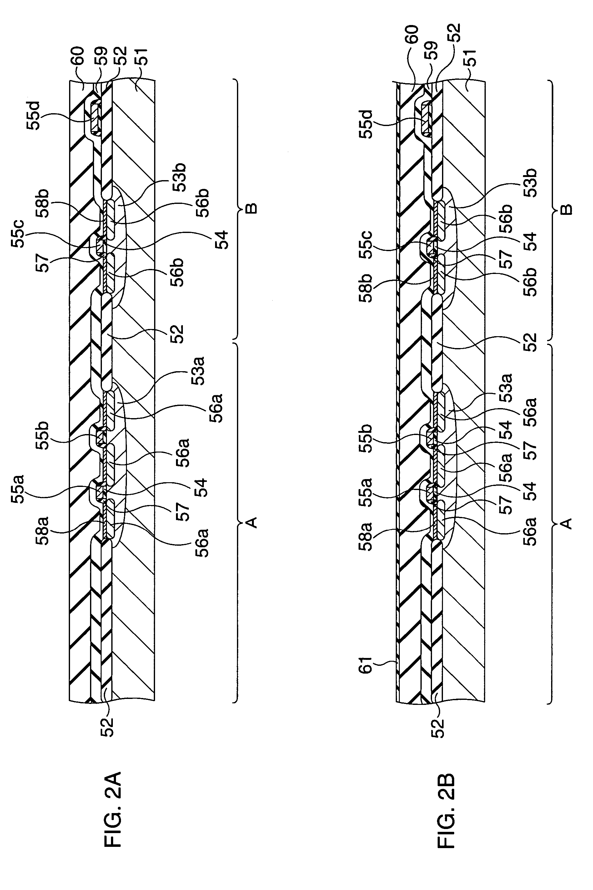
[0031]Next, a first embodiment of the present invention will be explained. FIG. 2A to FIG. 2R are sectional views showing a manufacturing method of the ferroelectric memory (semiconductor device) according to the first embodiment of the present invention.

[0032]In this embodiment, a device isolation insulating film 52 is first formed on a surface of a silicon substrate 51, first, as shown in FIG. 2A. Next, a p-well 53a and an n-well 53b are formed by selectively introducing a p-type impurity and an n-type impurity, respectively into predetermined active regions (transistor forming regions) in a memory cell region A and a peripheral circuit region B. A conductive type of the silicon substrate 51 may be either the p-type or the n-type. Next, a silicon oxide film is formed as a gate insulating film 54 by thermally oxidizing surfaces of the active regions of the silicon substrate 1. Then, an amorphous or a polycrystalline silicon film is formed on an entire upper surface of the silicon s...

second embodiment

[0071]Next, a second embodiment of the present invention will be explained. FIG. 3A to FIG. 3G are sectional views showing a manufacturing method of a ferroelectric memory (semiconductor device) according to the second embodiment of the present invention in the sequence of the process steps.

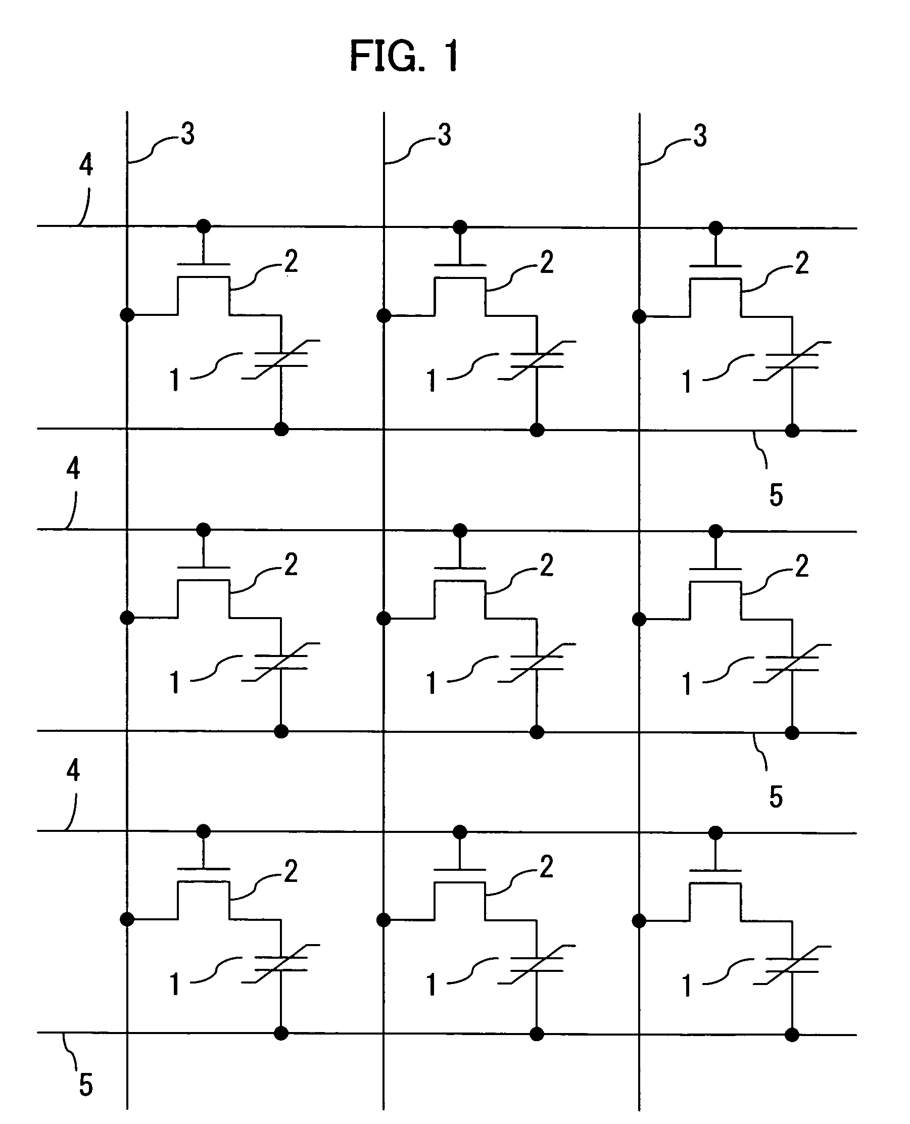
[0072]First, as shown in FIG. 3A, device isolation regions 12 are formed on a surface of a semiconductor substrate 11 such as a silicon substrate by, for example, STI (shallow trench isolation). Next, in a device active region which is partitioned by the device isolation regions 12, a well 13 is formed on the surface of the semiconductor substrate 11. Subsequently, a gate insulating film 17, a gate electrode 18, a silicide layer 19, source / drain diffusion layers 15, side walls 20 and silicide layers 16 are formed on a surface of the well 13, whereby a MOS transistor 14 is formed. The MOS transistor 14 corresponds to the MOS transistor 2 in FIG. 1. Two source / drain diffusion layers 15 are formed i...


PUM

PropertyMeasurementUnit
temperatureaaaaaaaaaa
thicknessaaaaaaaaaa
thicknessaaaaaaaaaa

Abstract

An IrOx film is formed as a first conductive oxide film on a PLZT film by a reactive sputtering method. Thereafter, thermal treatment by, for example, RTA is performed in an atmosphere containing oxygen having partial pressure of less than 5% of atmospheric pressure. As a result, crystallization of the PLZT film is promoted, and annealing treatment is performed for the IrOx film. Thereafter, furnace annealing at 600° C. or higher, for example, 650° C. is performed for 60 minutes in, for example, an O2 atmosphere as recovering annealing to recover oxygen deficiency in the PLZT film. Subsequently, an IrO2 film is formed as a second conductive oxide film on the IrOx film by a sputtering method.

Description

CROSS-REFERENCE TO RELATED APPLICATIONS[0001]This application is based upon and claims the benefit of priority from the prior Japanese Patent Application No. 2003-425785, filed on Dec. 22, 2003, the entire contents of which are incorporated herein by reference.BACKGROUND OF THE INVENTION[0002]1. Field of the Invention[0003]The present invention relates to a manufacturing method of a semiconductor device suitable for a ferroelectric memory.[0004]2. Description of the Related Art[0005]A flash memory and a ferroelectric memory are known, as a nonvolatile memory that can still store information after the power supply is turned off.[0006]In the flash memory, a floating gate is buried in a gate insulating film of an insulated-gate field effect transistor (IGFET), and information is stored by accumulating electric charges expressing memory information in the floating gate. A tunnel current that passes through the insulating film has to be passed to write and erase the information, and thus...

Claims


Application Information

Patent Timeline
Patent Type & Authority Patents(United States)
IPC IPC(8): H01L21/00H01L21/8234H01L21/02H01L21/8246H01L27/088H01L27/10H01L27/105H01L27/108H01L27/115H01L29/76H01L29/94H01L31/119
CPCH01L27/11502H01L28/65H01L28/57H01L27/11507H10B53/30H10B53/00
Inventor MATSUURA, KATSUYOSHIWANG, WENSHENGNAKAMURA, KO
Owner FUJITSU SEMICON LTD
Why Eureka
Try Eureka