Thermal flux deposition by scanning

a scanning and flux technology, applied in the direction of manufacturing tools, solid-state diffusion coating, welding/soldering/cutting articles, etc., can solve the problems of exposing the substrate to elevated temperatures for too long, slow ramping of the temperature of the substrate, etc., to reduce the total radiated power requirement, and accelerate the decomposition of reactants

Inactive Publication Date: 2006-07-18
APPLIED MATERIALS INC
View PDF36 Cites 35 Cited by
  • Summary
  • Abstract
  • Description
  • Claims
  • Application Information

AI Technical Summary

Benefits of technology

[0030]Still further, there is provided a method for thermally processing a substrate. A continuous wave of radiation is focused into a line of radiation at an upper surface of the substrate. The line of radiation is translated relative to the surface at a constant predetermined speed. This allows for every point of the substrate to have a substantially homogenous thermal exposure or history. Process control is achieved by modulating scan speed rather than lamp power, thereby simplifying the control of the apparatus. This allows for highly local heating without generating defects.
[0031]Therefore, the present invention heats only a small portion of the surface of the substrate at any given moment. This reduces the total radiated power requirement. In fact, an energy density of 150 kW / cm2 is achievable on a 300 mm substrate from a 5 kW radiation source.
[0033]The above described apparatus and method can heat the substrate surface to any temperature for a millisecond or less. In addition, as the line of radiation only applies heat to the surface of the substrate, the reaction of the gasses only occurs at the surface. This allows, multiple gasses to be injected simultaneously without leading to undesirable gas phase reactions away from the substrate surface. This method can be performed at atmospheric pressure, resulting in faster decomposition of reactants, thereby enabling high deposition rates.

Problems solved by technology

While such processes are widely used, current technology is not ideal.
It tends to ramp the temperature of the substrate too slowly and expose the substrate to elevated temperatures for too long.
These problems become more severe with increasing substrate sizes, increasing switching speeds, and / or decreasing feature sizes.
A drawback of RTP is that it heats the entire substrate even though the IC devices reside only in the top few microns of the substrate.
This limits how fast one can heat up and cool down the substrate.
Moreover, once the entire substrate is at an elevated temperature, heat can only dissipate into the surrounding space or structures.
As a result, today's state of the art RTP systems struggle to achieve a 400° C. / s ramp-up rate and a 150° C. / s ramp-down rate.
However, the laser pulse or flash used for laser annealing is too fast and, often does not provide enough time for sufficient annealing to occur for non-melt processes.
Also, devices or structures next to the exposed regions may be exposed to extreme temperatures causing them to melt, or to temperatures that are too low resulting in too little annealing.
Still further, homogenization of the thermal exposure of each portion of the substrate is difficult to attain because different regions adsorb at different rates resulting in huge temperature gradients.
The process is too fast for thermal diffusion to equilibrate temperature, thereby creating severe pattern dependencies.
As a result, this technology is not appropriate for single crystal silicon annealing because different regions on the substrate surface may be heated to vastly different temperatures causing large non-uniformities over short distances.
Reactions occurring in the ambient space are undesirable as they tend to form small particles of the desired material which do not adhere well to the surface of the substrate.
This may result in a non-uniform layer or a layer with numerous defects.
However, current thermally driven processes heat the entire substrate, despite the fact that only the surface of the substrate needs to be heated.
Heating the entire substrate limits how fast one can heat up and cool down the substrate, as the substrate has a thermal inertia that resists changes in temperature.
However, deposition rates for ALD are slow, taking approximately 1 Angstrom per second.
Also, ALD is bound by the same temperature constraints and thermal budget issues as CVD.

Method used


Image

  • Thermal flux deposition by scanning
  • Thermal flux deposition by scanning
  • Thermal flux deposition by scanning

Examples


Embodiment Construction

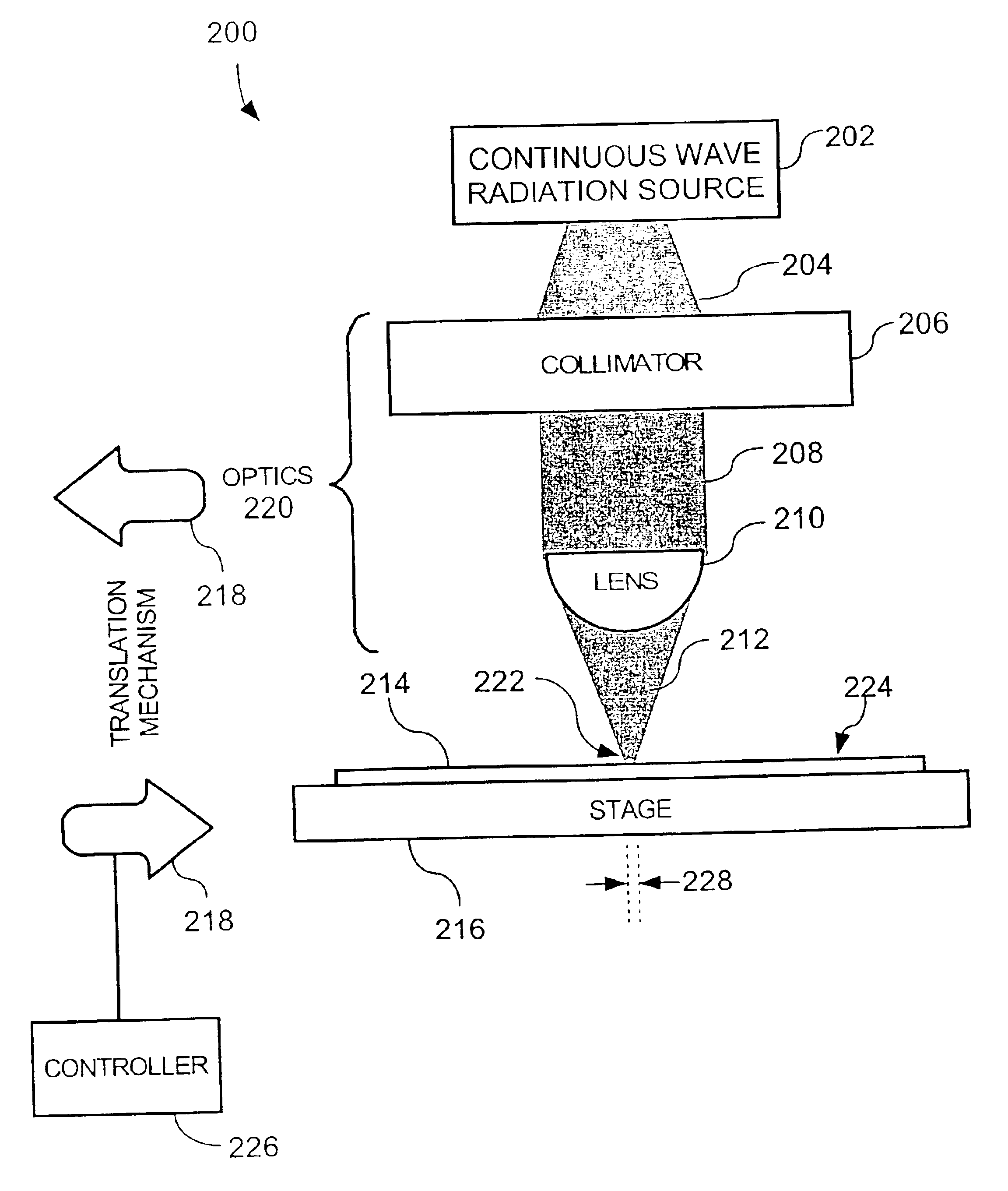
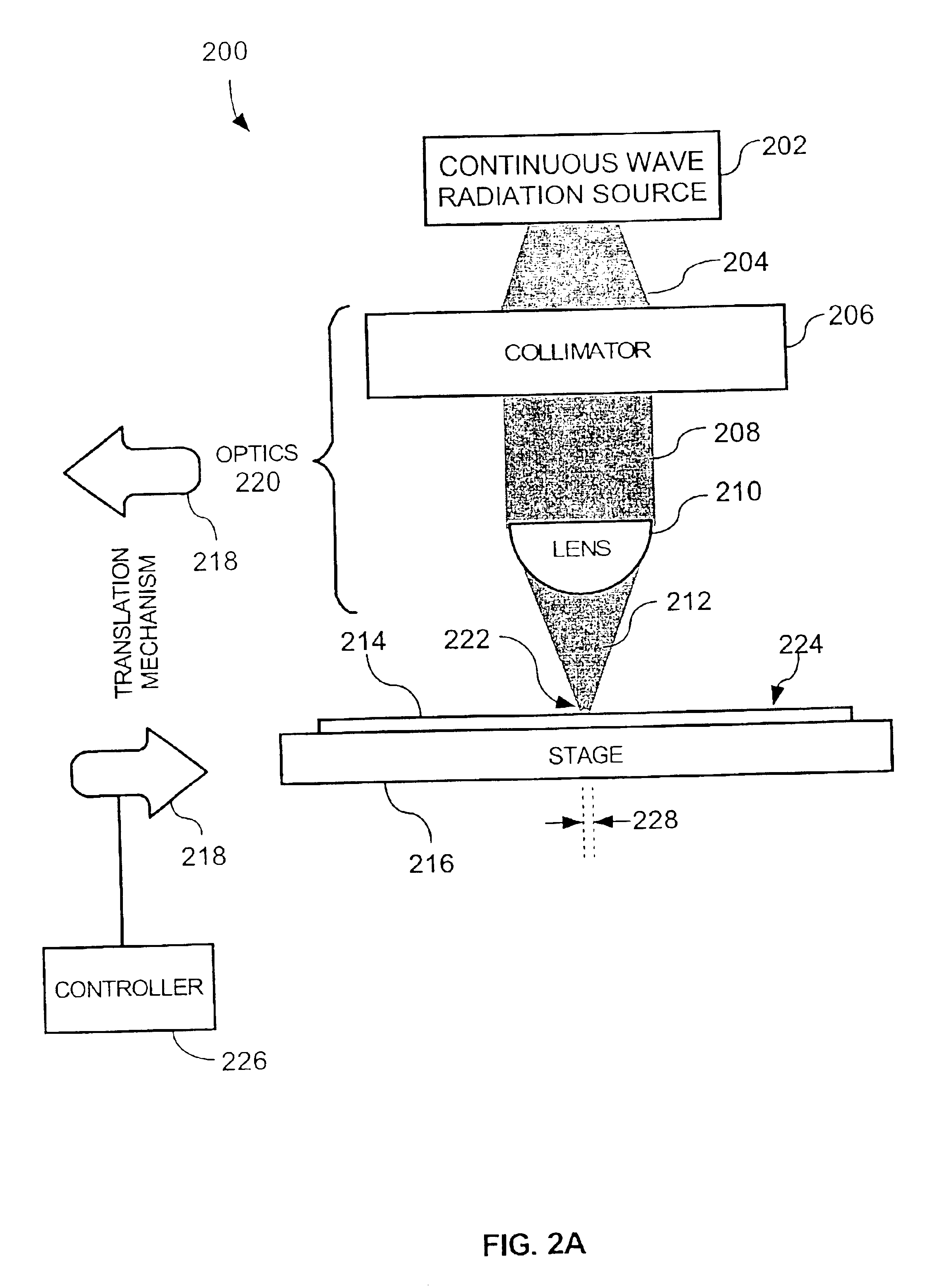
[0045]FIG. 2A is a side view of an apparatus 200 for thermally processing a substrate, according to an embodiment of the invention. The thermal process is any thermal process that requires the characteristics of the invention described below. Exemplary embodiments of such a thermal process includes thermal annealing of substrates or thermal processes used in Chemical Vapor Deposition (CVD), both of which will be described throughout the remainder of the Figures.

[0046]The apparatus 200 comprises a continuous wave electromagnetic radiation source 202, a stage 216 configured to receive a substrate 214 thereon, and optics 220 disposed between the continuous wave electromagnetic radiation source 202 and the stage 216.

[0047]In a preferred embodiment, the substrate 214 is any suitable substrate, such as a single crystal silicon substrate; silicon on insulator (SOI); Silicon Germanium or alloys thereof; glass or quartz substrate with a silicon layer thereon, as used for manufacturing thin f...


PUM

PropertyMeasurementUnit
poweraaaaaaaaaa
poweraaaaaaaaaa
poweraaaaaaaaaa

Abstract

A substrate is initially positioned in the reaction chamber. One or more gases are introduced into the reaction chamber. A predetermined speed for translating a line of radiation is determined. Continuous wave electromagnetic radiation is then emitted from a continuous wave radiation source. The continuous wave electromagnetic radiation is subsequently focused into a line of radiation extending across the surface of the substrate. The line of radiation is then translated relative to the surface at the constant predetermined speed. The combination of the introduced gas / es and heat generated by the line of radiation causes the gas / es to react and deposit a layer on the surface of the substrate. Undesirable byproducts of the reaction are then flushed from the reaction chamber. This process is repeated until a layer having a predetermined thickness is formed on the surface of the substrate.

Description

[0001]This application claims priority to, and is a continuation-in-part of, U.S. patent application entitled “THERMAL FLUX PROCESSING BY SCANNING,” having Ser. No. 10 / 126,419, and filed on Apr. 18, 2002, which is hereby incorporated by reference.BACKGROUND OF THE INVENTION[0002]1. Field of the Invention[0003]The invention relates generally to semiconductor device manufacture. More particularly, the invention is directed to an apparatus and method for depositing one or more layers on a substrate using a line of electromagnetic radiation. Furthermore, the invention is directed to an apparatus and method for thermally processing a substrate by scanning the substrate with a line of radiation.[0004]2. Description of Related Art[0005]The integrated circuit (IC) market is continually demanding greater memory capacity, faster switching speeds, and smaller feature sizes. One of the major steps the industry has taken to address these demands is to change from batch processing a substrate, su...

Claims


Application Information

Patent Timeline
Patent Type & Authority Patents(United States)
IPC IPC(8): B23K26/08B23K26/03B23K26/06B23K26/12B23K26/34C23C8/00C23C8/10C23C8/22C23C16/04C23C16/48H01L21/20
CPCB23K26/03B23K26/3266B23K26/0665B23K26/0807B23K26/083B23K26/0838B23K26/123B23K26/34C23C8/00C23C8/10C23C8/22C23C16/047C23C16/481H01L21/2026B23K26/0652B23K26/0643B23K2201/40B23K26/082B23K26/32B23K2101/40B23K2103/50H01L21/02683H01L21/02678H01L21/02422H01L21/0242H01L21/02381H01L21/02691H01L21/0262H01L21/02532
Inventor JENNINGS, DEAN
Owner APPLIED MATERIALS INC
Why Eureka
Try Eureka