Method for detecting gas with the use of photocurrent amplification and the like and gas sensor

a technology of photocurrent amplification and gas sensor, which is applied in the direction of individual semiconductor device testing, semiconductor/solid-state device testing/measurement, instruments, etc., can solve the problems of difficult to achieve accurate measurement and drawback of slow response, so as to improve response speed and sensitivity.

Inactive Publication Date: 2006-07-25
JAPAN SCI & TECH CORP
View PDF11 Cites 5 Cited by
  • Summary
  • Abstract
  • Description
  • Claims
  • Application Information

AI Technical Summary

Benefits of technology

[0033]According to the present invention, using the sandwich cell formed by sandwiching an organic semiconductor between two metallic electrodes, a change in injection current associated with photocurrent multiplication or dark current multiplication at the organic / metallic interface is used for sensing gas, so that the absolute value of the sensed current becomes large and hence the sensitivity is improved. In addition, since a change in injection current is detected at the interface, the response speed can be improved.

Problems solved by technology

However, since the dark conductivity of the organic semiconductor is extremely small, and the current is measured by means of comb like electrodes of which electrode-to-electrode distance is normally about 100 μm, an absolute value of the detected current is very small in the order of nA (nano ampere), leading the drawback that it is difficult to achieve accurate measurement.
In addition, since the change in dark conductivity is measured by measuring a change in resistance of entire organic thin film bulk, diffusion of molecules into the film bulk is a rate-determining factor, so that the drawback of slow response also arises.

Method used


Image

  • Method for detecting gas with the use of photocurrent amplification and the like and gas sensor
  • Method for detecting gas with the use of photocurrent amplification and the like and gas sensor
  • Method for detecting gas with the use of photocurrent amplification and the like and gas sensor

Examples


first embodiment

[0045]The first embodiment will be described by way of an example where a p-type organic semiconductor is used.

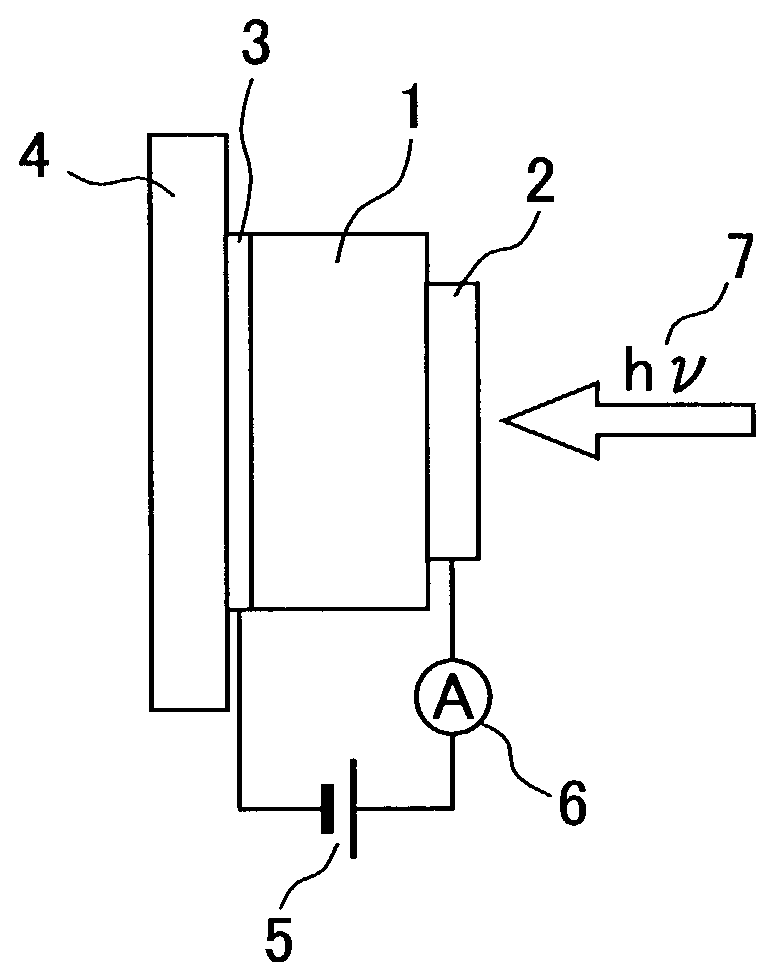
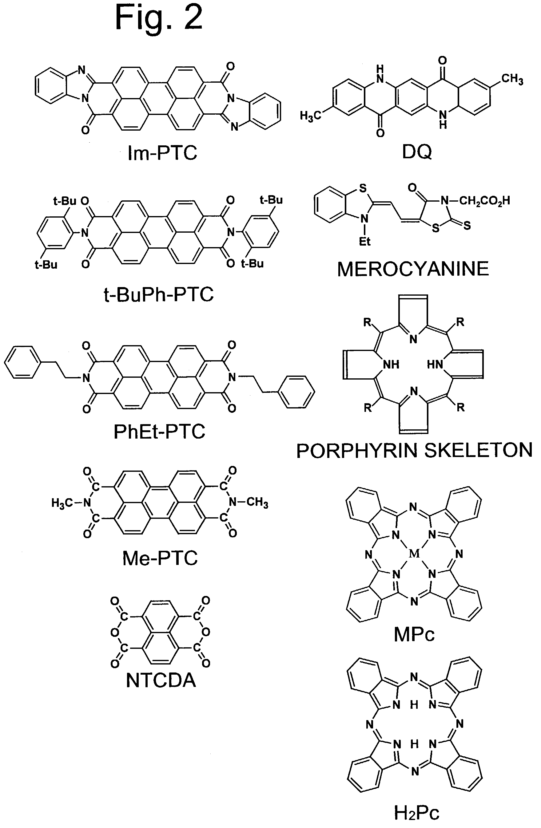
[0046]FIG. 1 is a schematic configuration view of a gas sensor device in which a section view of a sandwich cell structure of a photocurrent multiplication gas sensor device according to the first embodiment is shown together with an electric circuit. The reference numeral 1 denotes an organic semiconductor thin film which is a copper phthalocyanine (CuPc: the center metal M is Cu in the chemical formula represented as MPc in FIG. 2) evaporated film having a film thickness of about 1,000 nm. The reference numeral 2 denotes a metallic electrode thin film which is formed on one surface of the organic semiconductor film 1 so as to closely contact with the same, which is an In (indium) evaporated film having a film thickness of about 100 nm. The reference numeral 3 denotes another metallic electrode thin film which is an Au (gold) evaporated film having a film thickness of abou...

second embodiment

[0064]As the second embodiment, FIG. 8 shows an example wherein an n-type organic semiconductor is used. As an organic semiconductor thin film 1a, a perylene pigment (Me-PTC: represented by the chemical formula in FIG. 2) evaporated film having a film thickness of about 500 nm or a naphthalene derivative (NTCDA: represented by the chemical formula in FIG. 2) evaporated film having a film thickness of about 500 nm, which exhibits n-type semiconductor property, is used. As a metallic electrode 2a on the side where a gas to be sensed comes into contact and light is irradiated, an Au evaporated film having a film thickness of about 20 nm is used, and as the other metallic electrode 3a, an ITO (indium tin oxide) evaporated film having a film thickness of about 60 nm is used.

[0065]In the case of the n-type semiconductor, the photocurrent multiplication phenomenon occurs at the interface between the electrode to which the voltage is negatively applied and the organic semiconductor (as will...


PUM

PropertyMeasurementUnit
thicknessaaaaaaaaaa
thicknessaaaaaaaaaa
thicknessaaaaaaaaaa

Abstract

An indium electrode film (2) is formed closely adhering to one face of an organic semiconductor film (1) made of copper phthalocyanine while a gold electrode film (3) is formed on the other face. A voltage is applied to the organic semiconductor film (1) so that the indium electrode (2) side is biased positively. By applying a voltage so that the electrode (2) side is charged positively and irradiating with a light having a wavelength absorbable by the organic semiconductor film (1) the phenomenon of photocurrent multiplication arises at the interface of the organic semiconductor film (1) and the electrode (2). When put under an oxygen or moisture atmosphere in the above state, this gas sensor can detect oxygen or moisture depending on a change in photocurrent due to the multiplication.

Description

TECHNICAL FIELD[0001]The present invention relates to a method for sensing atmospheric gas using a cell having an organic semiconductor film, and to a gas sensor implementing this method.BACKGROUND ART[0002]Conventionally, as a gas sensor using an organic semiconductor, semiconductor gas sensors of the electric resistance type wherein comb like electrodes are formed on the surface of an organic semiconductor film and gas concentration is sensed using the fact that the dark conductivity of the organic semiconductor layer changes due to adsorption of gas have been generally used. As an example of such a gas sensor, NO2 sensors using a change in dark conductivity of a phthalocyanine-based thin film are known (See M. Passard, A. Pauly, J. P. Germain, C. Maleysson, Synthetic Metals, 80, 25 (1996), for example.)[0003]On the other hand, the present invention is based on the photocurrent multiplication phenomenon occurring at an organic / metallic interface (See M. Hiramoto, T. Imahigashi, M....

Claims


Application Information

Patent Timeline
Patent Type & Authority Patents(United States)
IPC IPC(8): H01L21/66G01N27/416G01N25/56G01N27/00G01N27/12G01N33/00H01L31/10H01L51/00H01L51/30H01L51/42
CPCG01N25/56G01N27/002G01N27/126G01N33/0036H01L51/0078H01L51/0042H01L51/005H01L51/0053H10K85/146H10K85/60H10K85/621H10K85/311
Inventor HIRAMOTO, MASAHIROYOKOYAMA, MASAAKIYOSHIDA, MANABU
Owner JAPAN SCI & TECH CORP
Why Eureka
Try Eureka