Fabrication method of semiconductor integrated circuit device

a technology of integrated circuits and fabrication methods, which is applied in the direction of transistors, basic electric elements, chemistry apparatuses and processes, etc., can solve the problems of increasing the resistance of buried interconnects, conspicuously short life of tddb (time dependent on dielectric breakdown), and difficulty in securing sufficient tddb life, so as to prevent an increase in the resistance of an interconnect, improve the adhesion, and improve the effect of dielectric breakdown

Inactive Publication Date: 2006-08-01
HITACHI LTD
View PDF28 Cites 31 Cited by
  • Summary
  • Abstract
  • Description
  • Claims
  • Application Information

AI Technical Summary

Benefits of technology

[0017]It is an object of the invention to provide a technique which is capable of improving the dielectric breakdown strength between interconnects having copper in the main conductor layers thereof.
[0018]Another object of the invention is to provide a technique which is capable of preventing an increase in the resistance of an interconnect having copper main-conductor layer.
[0019]Another object of the invention is to provide a technique to improve the adhesion between an interconnect having a copper main conductor layer and a cap film.

Problems solved by technology

Firstly, there exists a problem in that, when using copper as an interconnect material, the TDDB (Time Dependence on Dielectric Breakdown) life is conspicuously short as compared to other metal materials (e.g. aluminum, tungsten).
However, because the low-dielectric-constant dielectric material generally is low in dielectric strength, there is still more difficulty in securing sufficient a TDDB life.
Secondly, if a silicon nitride film is used as a cap film on a buried interconnect having a copper main-conductor layer, silicide or copper oxide is formed at the interface of the copper and the silicon nitride film during formation of a cap film, causing a problem of increased resistance of the buried interconnect.

Method used


Image

  • Fabrication method of semiconductor integrated circuit device
  • Fabrication method of semiconductor integrated circuit device
  • Fabrication method of semiconductor integrated circuit device

Examples


embodiment 1

[0149]An explanation will now be given of the problem in a post-CMP cleaning technique studied by the present inventors and the means for solving such problem.

[0150]The post-CMP cleaning technique studied by the present inventors is designed to carry out alkali cleaning and acid cleaning in this order on a semiconductor substrate after CMP processing. Alkali cleaning has an object to remove foreign matter, such as the slurry used during CMP processing. In alkali cleaning, a cleaning liquid containing, for example, ammonia (NH4OH) is used. Also, acid cleaning has an object to improve the TDDP characteristic or remove the remaining metal. In acid cleaning, a cleaning liquid containing, for example, hydrogen fluoride (HF) is used.

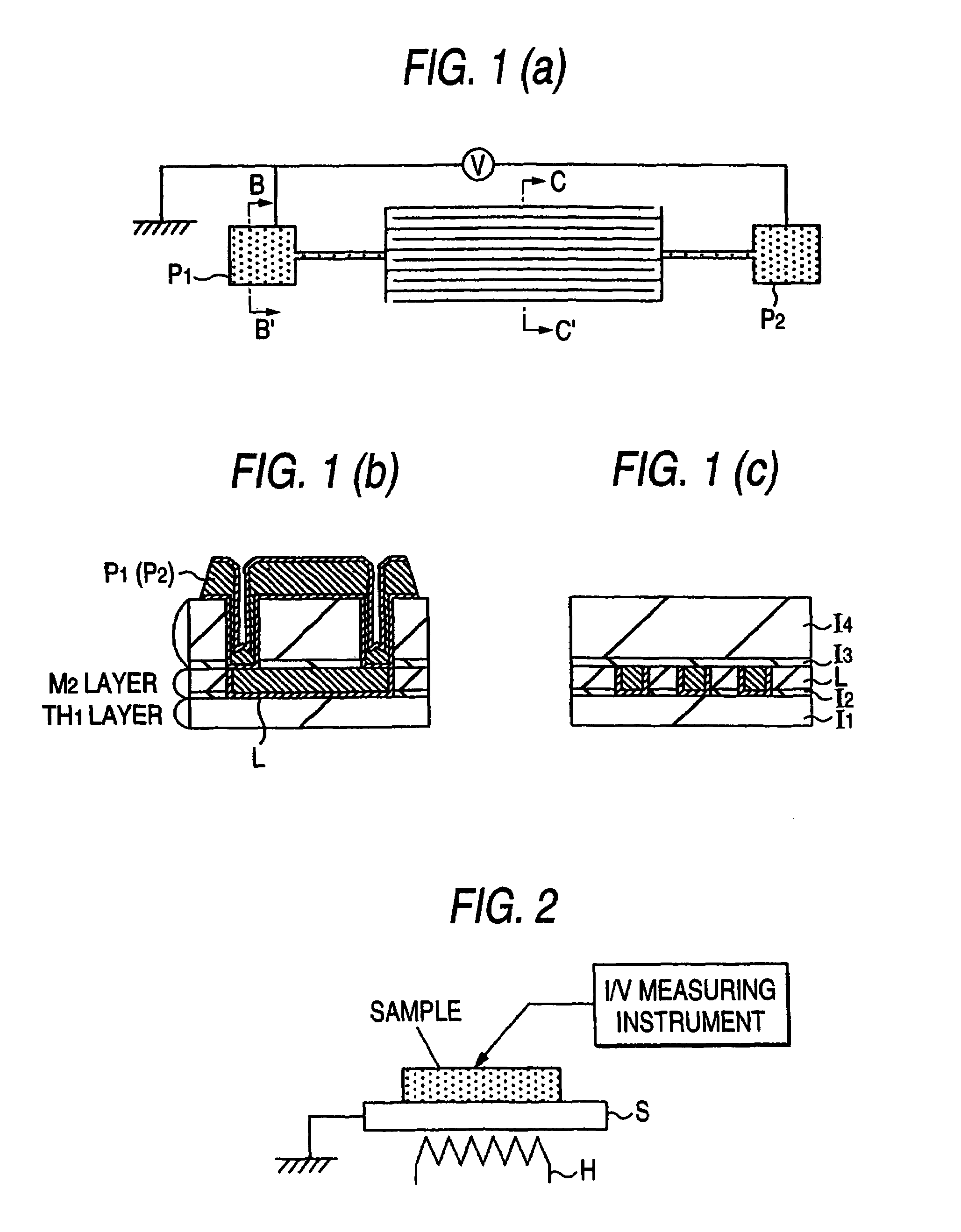
[0151]FIGS. 5(a) and 5(b) show respective examples of sections in the buried interconnects 65a, 65b in which a cleaning process is carried out on buried interconnects that are different in interconnect dimensions. The buried interconnects 65a, 65b are formed i...

embodiment 2

[0268]The present embodiment is directed to a modification of the foregoing post-CMP cleaning process.

[0269]FIG. 43 is a flowchart illustrating this modification. An example is herein given of the case of carrying out the foregoing deoxiding process (step 106) after the CMP process (step 104), and thereafter performing a post-cleaning process in the order of alkali cleaning (step 105) and acid cleaning (step 107). The other points of the process are similar to those of the Embodiment 1. In this case, a similar effect to the post-CMP cleaning process is obtained. In this case, a deoxidization processing section may be provided in the CMP apparatus.

[0270]Meanwhile, FIG. 44 is a flowchart of another example of a post-CMP cleaning process. An example is herein given of the case in which the invention is applied where acid cleaning only is carried out without performing alkali cleaning. The other features are similar to those of the Embodiment 1. The TDDB characteristic is improved by me...

embodiment 3

[0271]The present embodiment is directed to a modification of the foregoing post process.

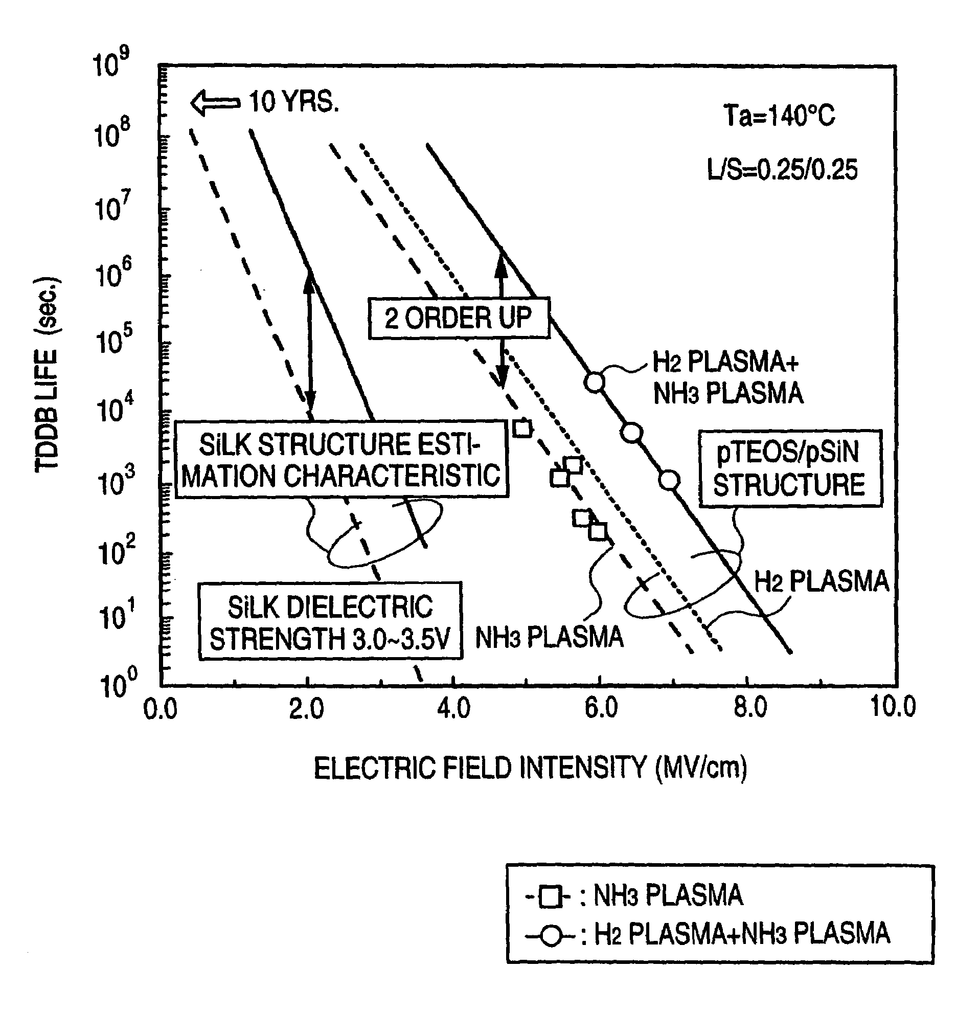
[0272]FIG. 45 shows a part of the flowchart illustrating the process. An example is herein given of the case in which, after an ammonia plasma process, a hydrogen plasma process is continuously carried out while maintaining a vacuum. The other features are similar to those of the Embodiments 1 and 2. Meanwhile, FIG. 46 exemplifies a case in which an ammonia plasma process only is carried out in a post process. The other features are similar to those of the Embodiments 1 and 2. In these cases, the TDDB characteristic could have been improved despite the fact that the interconnect resistance has decreased to a level lower than that of the Embodiments 1 and 2.


PUM

PropertyMeasurementUnit
dielectric constantaaaaaaaaaa
thicknessaaaaaaaaaa
temperatureaaaaaaaaaa

Abstract

The copper interconnect formed by the use of a damascene technique is improved in dielectric breakdown strength (reliability). During post-CMP cleaning, alkali cleaning, a deoxidizing process due to hydrogen annealing or the like, and acid cleaning are carried out in this order. After the post-CMP cleaning and before forming an insulation film for a cap film, hydrogen plasma and ammonia plasma processes are carried out on the semiconductor substrate. In this way, a copper-based buried interconnect is formed in an interlayer insulation film structured of an insulation material having a low dielectric constant.

Description

[0001]This application is a Continuation application of application Ser. No. 09 / 965,220, filed Sep. 28, 2001 now U.S. Pat. No. 6,723,631, the contents of which are incorporated herein by reference in their entirety.BACKGROUND OF THE INVENTION[0002]This invention relates to a method of fabrication of a semiconductor integrated circuit device; and, more particularly, the invention relates to a technique applicable effectively to a method of fabrication of a semiconductor integrated circuit device having buried interconnects with copper in the main conductor layers thereof.[0003]In semiconductor integrated circuit devices, electronic devices, etc., a technique has been established to form interconnects as an interconnect-forming technology, wherein a conductor film, e.g., aluminum or tungsten, is deposited on an insulation film, and then the film is patterned by the usual photolithography and dry-etch technique, thereby being formed into an interconnect.[0004]In the above interconnect-...

Claims


Application Information

Patent Timeline
Patent Type & Authority Patents(United States)
IPC IPC(8): H01L21/302H01L21/3205H01L21/02H01L21/28H01L21/304H01L21/321H01L21/3213H01L21/768H01L21/8234H01L23/522H01L23/532H01L27/088
CPCH01L21/02074H01L21/321H01L21/3212H01L21/76801H01L21/76808H01L21/76832H01L21/76838H01L21/76843H01L21/76849H01L21/76862H01L21/76864H01L21/76867H01L21/76883H01L2924/0002H01L21/32136H01L23/53238H01L2924/00H01L21/7684H01L21/28
Inventor NOGUCHI, JUNJIASAKA, SHOJIKONISHI, NOBUHIROOHASHI, NAOHUMIMARUYAMA, HIROYUKI
Owner HITACHI LTD
Why Eureka
Try Eureka